Theory of Operation—492/492P Service Vol. 1 (SN B030000 & up)
DATA BUFFER
c =
INPUT
REGISTER
CS0
RS0
CHIP SELECT
AND CONTROL
:>
CONTROL
REGISTER A
.
DATA
DIRECTION
REGISTER A
I
TO POLL
PERIPHERAL
INTERFACE A
ABtf- AB7
OUTPUT BUS
PERIPHERAL
INTERFACE B
DB0-DB7
0
DATA
DIRECTION
I
t
CONTROL
CB2
REGISTER B
TO DATA
VALID
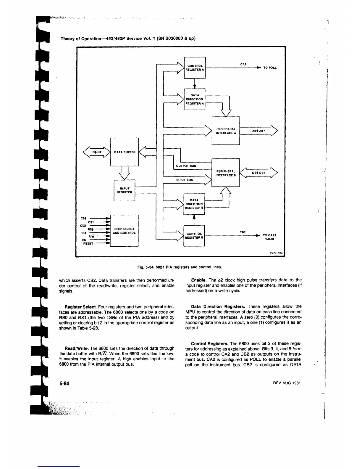
Fig. 5-34. 6821 PIA registers and control lines.
which asserts CS2. Data transfers are then performed un
der control of the read/write, register select, and enable
signals.
Register Select. Four registers and two peripheral inter
faces are addressable. The 6800 selects one by a code on
RSO and RS1 (the two LSBs of the PIA address) and by
setting or clearing bit 2 in the appropriate control register as
shown in Table 5-23.
Enable. The φ2 clock high pulse transfers data to the
input register and enables one of the peripheral interfaces (if
addressed) on a write cycle.
Data Direction Registers. These registers allow the
MPU to control the direction of data on each line connected
to the peripheral interfaces. A zero (0) configures the corre
sponding data line as an input; a one (1 ) configures it as an
output.
Read/Write. The 6800 sets the direction of data through
the data buffer with R/W. When the 6800 sets this line low,
it enables the input register. A high enables input to the
6800 from the PIA internal output bus.
Control Registers. The 6800 uses bit 2 of these regis
ters for addressing as explained above. Bits 3,4, and 5 form
a code to control CA2 and CB2 as outputs on the instru
ment bus. CA2 is configured as POLL to enable a parallel
poll on the instrument bus. CB2 is configured as DATA
5-84
REV AUG 1981



 To Next Page