492/492P Service Vol. I (SN B030000 & up)
LIST OF ILLUSTRATIONS
Fig.
No. Page
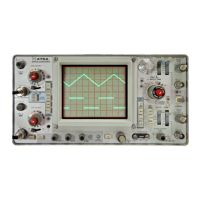
The 492/492P Spectrum Analyzer xii
1-1 Probe power connector pin o u t
................
1-12
1-2 Dimensions............................................... 1-14
1-3 International power cord and plug
configuration for the 492............................ 1-20
3-1 Test equipment setup for checking
frequency of the calibrator and the
accuracy of the frequency readout
............
3-8
3-2 Test equipment setup showing two methods
that check calibrator output level
..............
3-10
3-3 Test equipment setup for verifying
attenuator and gain accuracy.................... 3-12
3-4 Test equipment setup for checking the
10 kHz—10 MHz frequency response .... 3-16
3-5 Test equipment setup for measuring the
0.01—2.0 GHz frequency response
..........
3-17
3-6 Typical display showing frequency response
from a sweeping signal source
.................. 3-17
3-7 Test equipment setup for measuring 2.0—
18.0 GHz frequency response.................... 3-19
3-8 Test equipment setup for checking span and
timing accuracy
......................................... 3-21
3-9 Display to illustrate how timing accuracy
is checked................................................. 3-22
3-10 Measuring resolution bandwidth and
shape factor
............................................. 3-24
3-11 Typical display of drift measurement without
phaselock showing width of marker stored
with MAX HOLD and beginning display of
marker saved in A
.....................................
3-27
3-12 Displays that illustrate how to measure resid
ual FM with PHASELOCK off. The same
technique is used with PHASELOCK on (Op
tion 03)..................................................... 3-27
3-13 Test equipment setup for measuring
intermodulation distortion.......................... 3-28
3-14 Intermodulation products.......................... 3-28
3-15 Test equipment setup to check harmonic
distortion................................................... 3-29
3-16 Typical display of phaselock noise
............
3-30
3-17 Multiple exposure to illustrate how the
differential between two signals can be
measured................................................... 3-31
3-18 Test equipment setup for checking triggering
requirements............................................. 3-32
3-19 Test equipment setup to check external
triggering and horizontal input
characteristics........................................... 3-33
vi
Fig.
No. Page
3-20 Test oscilloscope display of a sinewave
input signal to EXT TRIG connector (input
1.0 V peak at 2.0 V peak-to-peak)
............ 3-33
3-21 Display of a full screen signal at the
Vertical Output Connector
.........................
3-34
3-22 Low voltage power supply adjustments
and test point locations
.............................
3-44
3-23 Adjustments and test points on the
deflection amplifier, High Voltage module,
and Z-Axis/RF Interface board.................. 3-45
3-23 Location of wire strap (W4036) on high
voltage circuit board
.................................
3-45
3-25 Test equipment setup for calibrating the
Deflection Amplifier
................................... 3-46
3-26 Location of TP1101 on Crt Readout
........
3-47
3-27 Test points and adjustments on the
Deflection Amplifier board for gain and
frequency response calibration
.................
3-47
3-28 Test equipment setup for calibrating sweep
timing
........................................................
3-48
3-29 Location of timing adjustment R5105 and
TP1061 on sweep board
...........................
3-49
3-30 Test equipment setup for calibrating
sweep ramp for the 1 st LO Driver............ 3-50
3-31 1st LO balance and span adjustments and
test points................................................. 3-51
3-32 Test equipment setup for check and
adjustment of 1 st and 2nd LO frequencies. 3-54
3-33 Center Frequency Control adjustment
locations................................................... 3-55
3-34 1 st LO Driver adjustments and test point
locations................................................... 3-57
3-35 Test equipment setup for adjusting baseline
leveling....................................................... 3-58
3-36 Adjustments and test points on the Video
Processor board....................................... 3-59
3-37 Typical response displays when adjusting
baseline leveling
....................................... 3-60
3-38 Typical response displays when adjusting
compensation of baseline leveling circuits . 3-60
3-39 Equipment setup for calibrating log
amplifier
....................................................
3-61
3-40 Location of connectors and adjustments on
the Log and Video Amplifier
.....................
3-62
3-41 Test equipment setup for calibrating the
VR section................................................. 3-64
3-42 Calibration adjustments on the VR #2
module....................................................... 3-64
REV AUG 1981
 Loading...