Do you have a question about the Terasic de10-nano and is the answer not in the manual?
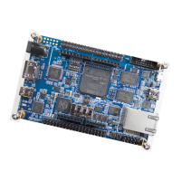
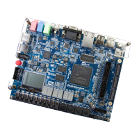
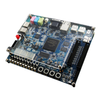
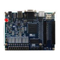
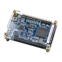
Identifies and shows the location of key connectors and components on the DE10-Nano board.
Presents a high-level block diagram illustrating the DE10-Nano board's architecture.
Explains how to set the FPGA configuration mode using DIP switches.
Details the JTAG and Active Serial (AS) programming methods for the FPGA.
Details interfaces connected to the FPGA, allowing user logic control.
Details the connections and functionality of push-buttons, switches, and LEDs on the FPGA side.
Describes the two 40-pin expansion headers and their pin assignments.
Explains the Arduino Uno R3 compatibility expansion header and its pin assignments.
Details the 8-channel, 12-bit A/D converter and its analog input connections.
Introduces interfaces connected to the HPS section of the Cyclone V SoC FPGA.
Describes the 1GB DDR3 SDRAM, its connections, and pin assignments.
Details how to control LEDs by writing to the PIO core registers.
Guides on executing the ARM C program and observing LED behavior.
Explains the required MSEL settings for Active Serial (AS) mode.
Details the steps to convert a .sof file to a .jic file using Quartus II.
Guides on programming the EPCS device with a .jic file using Quartus Programmer.
Explains the procedure to erase the existing file in the EPCS device.
Describes EPCS programming using the nios-2-flash-programmer tool.
| Brand | Terasic |
|---|---|
| Model | de10-nano |
| Category | Motherboard |
| Language | English |