Do you have a question about the Terasic DE1-SOC and is the answer not in the manual?
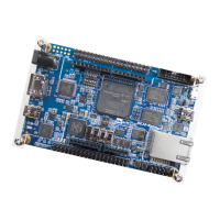
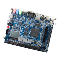
Details the hardware and accessories included in the DE1-SoC Development Kit.
Describes the contents of the DE1-SoC System CD, including manuals and designs.
Provides contact information and resources for obtaining technical assistance.
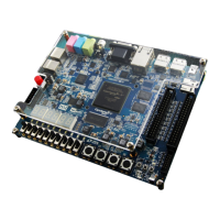
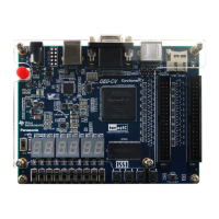
Illustrates the physical layout and identifies key components on the DE1-SoC board.
Presents a high-level block diagram showing the interconnections of the board's subsystems.
Explains how to select the FPGA configuration scheme using DIP switches.
Details the methods for programming the Cyclone V SoC FPGA via JTAG and AS modes.
Describes the LEDs and indicators that display the board's operational status.
Explains the function of the HPS cold and warm reset buttons.
Details the clock sources and distribution on the DE1-SoC board.
Introduces peripherals directly connected to the FPGA fabric.
Covers the functionality and pin assignments of user push-buttons, switches, and LEDs.
Details the six 7-segment displays and their FPGA pin assignments for output.
Describes the 2x20 GPIO headers for board expansion and their pin assignments.
Explains the 24-bit audio CODEC, its features, and connections.
Details the I2C multiplexer used for accessing peripherals.
Describes the VGA output interface, its DAC, and timing specifications.
Explains the TV decoder chip for video input and its interface.
Describes the infrared receiver module and its connection to the FPGA.
Details the infrared emitter LED and its connection to the FPGA.
Covers the 64MB SDRAM memory module and its pin assignments.
Explains the PS/2 interface for keyboard/mouse input and its pin assignments.
Details the 8-channel 12-bit ADC and its 2x5 header connections.
Introduces peripherals connected to the HPS section of the SoC.
Describes HPS-specific user push-buttons and LEDs and their control.
Explains the Gigabit Ethernet PHY and its connection and status LEDs.
Details the UART interface for HPS communication via USB.
Covers the 1GB DDR3 SDRAM connected to the HPS and its pin assignments.
Explains the Micro SD card interface for storage and booting.
Describes the USB 2.0 host ports and their interface controller.
Details the G-sensor module, its I2C interface, and connections.
Explains the 14-pin LTC connector for Linear Technology daughter cards.
Introduces the DE1-SoC System Builder tool for creating Quartus II projects.
Outlines the steps involved in using the DE1-SoC System Builder tool.
Provides detailed instructions on how to operate the DE1-SoC System Builder utility.
Demonstrates the default factory configuration of the DE1-SoC board.
Shows how to implement audio recording and playback using the CODEC.
Details how to create a Karaoke machine using audio ports and the CODEC.
Illustrates SDRAM access and verification using Nios II processor.
Demonstrates SDRAM testing using Verilog HDL and a system controller.
Explains how to turn the board into a TV box using video and audio peripherals.
Shows how to implement bi-directional communication with a PS/2 mouse.
Demonstrates the use of IR emitter LED and IR receiver for communication.
Illustrates the performance evaluation of the 8-channel 12-bit A/D Converter.
Guides on developing the first HPS program using Altera SoC EDS tool.
Shows how to control user LEDs and keys via HPS GPIO controller.
Explains how to control the G-sensor using the HPS I2C driver.
Demonstrates switching the I2C multiplexer for HPS to access the I2C bus.
Shows how HPS controls FPGA LEDs and HEX displays via Lightweight HPS-to-FPGA Bridge.
Demonstrates controlling HPS/FPGA peripherals and GUI programming on Linux.
Utilizes VGA as a standard output for Linux OS with frame buffer project.
Sets up the FPGA for programming the quad Flash configuration device.
Details the process of converting a .SOF file to a .JIC file in Quartus II.
Explains how to program the EPCS device using a created .JIC file.
Describes the steps to erase existing files from the EPCS device.
Provides guidance on booting from EPCS using Quartus II software.
Lists the changes and updates made in different versions of the manual.
Contains the copyright information and legal notices for the manual.
| FPGA Max. Memory | 4, 450 Kbits |
|---|---|
| Processor | Dual-core ARM Cortex-A9 (HPS) |
| Ethernet | 10/100/1000 Mbps |
| Switches | 4 |
| Push-buttons | 4 |
| HSMC (High-Speed Mezzanine Connector) | 1 |
| On-board USB Blaster | Yes |
| Clock Frequency | 50 MHz |
| Storage | MicroSD Card Slot |
| FPGA | Altera Cyclone V SoC (5CSEMA5F31C6) |
| Memory | 1GB DDR3 |
| USB | USB Host |
| HDMI | HDMI |
| Audio | 24-bit CODEC, Line-in, Line-out, Microphone |
| ADC | 12-bit ADC |
| Serial | UART |
| Video | VGA, HDMI |
| Power Supply | 5V |