LM2734
V
IN
V
IN
EN
BOOST
SW
FB
GND
V
OUT
C3
L1
C1
C2
R1
R2
D1
D2
ON
OFF
LM2734
SNVS288I –SEPTEMBER 2004–REVISED APRIIL 2013
www.ti.com
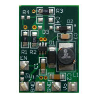
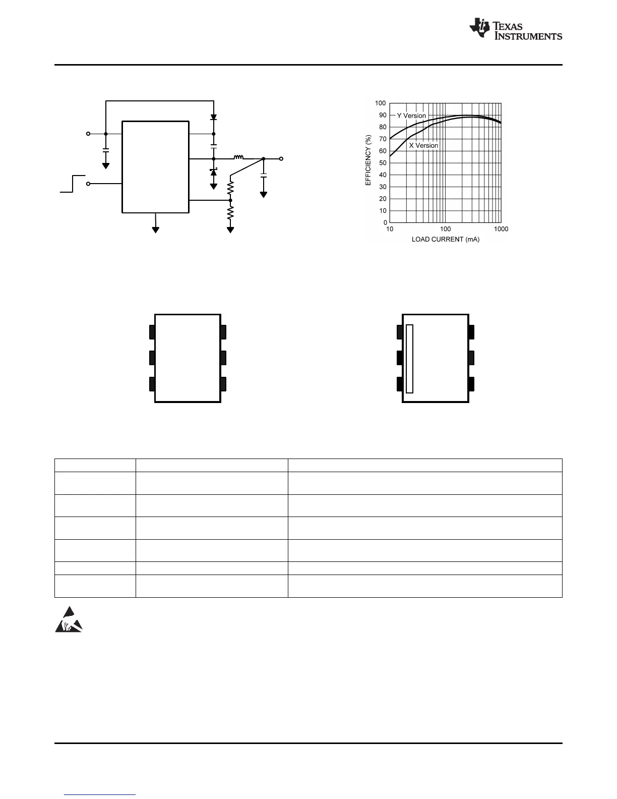
Typical Application Circuit
Figure 1. Figure 2. Efficiency vs Load Current
V
IN
= 5V, V
OUT
= 3.3V
Connection Diagram
Figure 3. 6-Lead SOT Figure 4. Pin 1 Indentification
See Package Number DDC (R-PDSO-G6)
PIN DESCRIPTIONS
Pin Name Function
1 BOOST Boost voltage that drives the internal NMOS control switch. A bootstrap
capacitor is connected between the BOOST and SW pins.
2 GND Signal and Power ground pin. Place the bottom resistor of the feedback
network as close as possible to this pin for accurate regulation.
3 FB Feedback pin. Connect FB to the external resistor divider to set output
voltage.
4 EN Enable control input. Logic high enables operation. Do not allow this pin to
float or be greater than V
IN
+ 0.3V.
5 V
IN
Input supply voltage. Connect a bypass capacitor to this pin.
6 SW Output switch. Connects to the inductor, catch diode, and bootstrap
capacitor.
These devices have limited built-in ESD protection. The leads should be shorted together or the device placed in conductive foam
during storage or handling to prevent electrostatic damage to the MOS gates.
2 Submit Documentation Feedback Copyright © 2004–2013, Texas Instruments Incorporated
Product Folder Links: LM2734