LB
R
LOAD
R
L
V
in
V
out
R
D S_ON
V
sense
R
D1
RD 2
CP
1
Gate
driver
Iref
Analog - to
- PWM
Gain =
1
PID
Compensator
K
P, KI, KD,
and T
s
R
S
R 3
R
4
C
P2
m f MIN(pk)
K 0.5 K V= ´ ´
( ) ( )
REF m m v f IN
2
RMS
1
I K A C B K U K V
V
æ ö
ç ÷
= ´ ´ ´ = ´ ´ ´ ´
ç ÷
è ø
www.ti.com
Digital PFC Description
12.8.1 Average Current Mode Control
The current loop is shown in the dashed line of Figure 38. The current reference signal I
REF
is calculated
as:
where
• Km – multiplier gain
• A – voltage loop output
• B – 1/(V
IN(rms)
)2
• C – V
IN
(1)
For sine wave input, the multiplier gain K
m
is expressed as,
(2)
In Figure 27, Ks and Kf are scaling factors. For further detail, please refer to reference , and .
12.8.2 ZVS and Valley Control
Please refer to the reference and .
12.9 Current Feedback Control Compensation Using PID Control
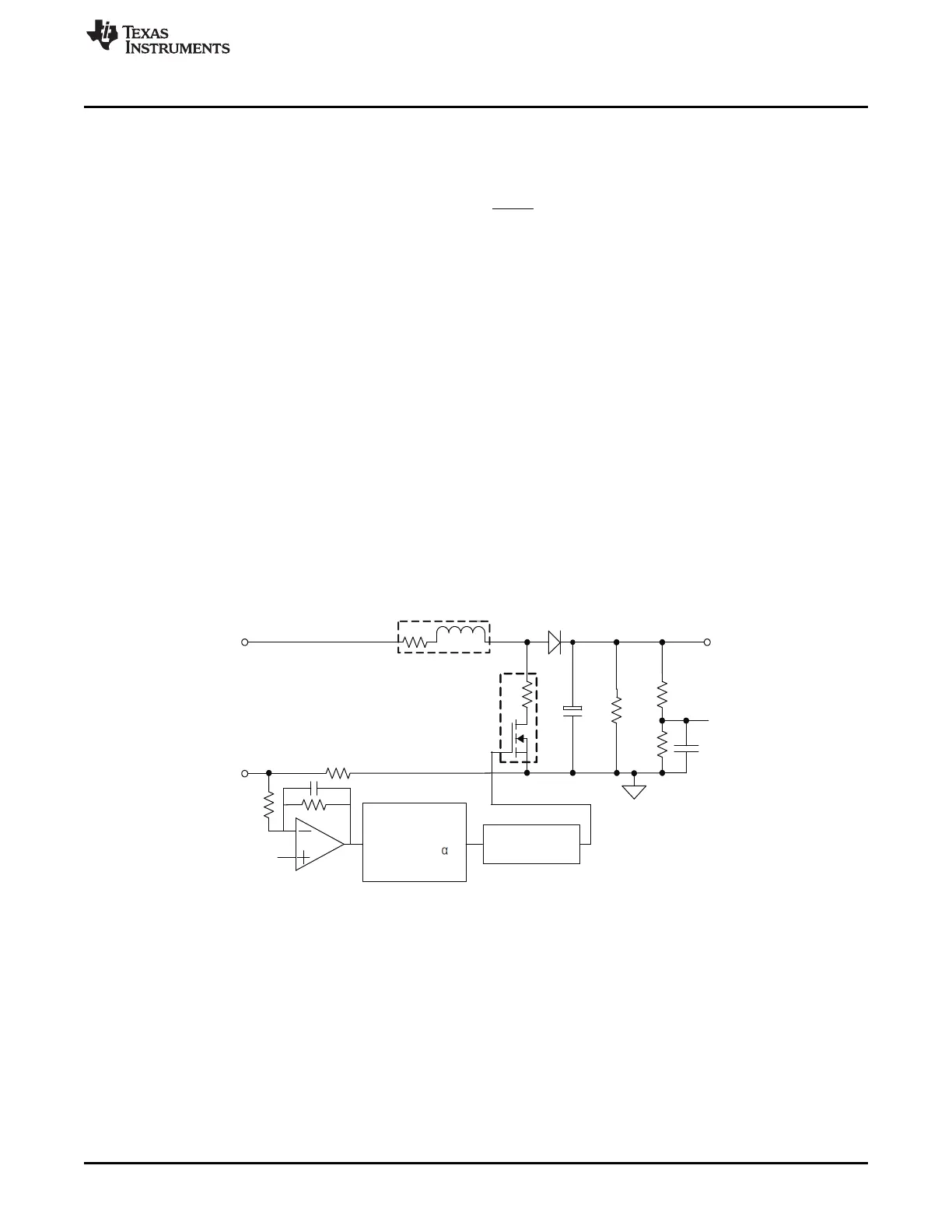
A functional block diagram of single-phase PFC control loop is shown in Figure 39.
PID control is usually used in the feedback loop compensation in digitally controlled power converters.
Described below are several aspects using PID control in the single-phase PFC feedback control loop.
Figure 39. Single-phase PFC Feedback Loop Using PID Control
41
SLUU885B–March 2012–Revised July 2012 Digitally Controlled Single-Phase PFC Pre-Regulator
Submit Documentation Feedback
Copyright © 2012, Texas Instruments Incorporated