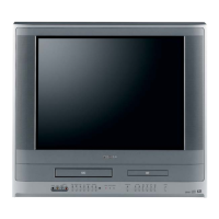
8-3
2-3 V Output
(1) Circuit Operation
The V output circuit consists of a V driver circuit IC302,
Pump-up circuit and output circuit IC301, and external
circuit components.
Q2 amplifies its input fed from pin 4 of IC301. Q3, Q4
output stage connected in a SEPP amplifies the current
and supplies a sawtooth waveform current and supplied
Fig. 6 Output stage operation waveform
a sawtooth waveform current to a deflection yoke. Q3 turns
on for first half of the scanning period and allows a positive
current to flow into the deflection yoke (Q3 DY C306
R305 GND), and Q4 turns on for last half of the
scanning period and allows a negative current to flow into
the deflection yoke (R305 C306 DY Q4). These
operations are shown in Fig. 5.
Fig. 5 V output circuit
In Fig. 6 (a), the power Vcc is expressed as a fixed level,
and the positive and negative current flowing into the
deflection yoke is a current (d) = current (b) + (c) in Fig.
6, and the emitter voltage of Q3 and Q4 is expressed as
(e).
Q3 collector loss i1 x Vce1 and the value is equal to
multiplication of Fig. 6 (b) and slanted section of Fig. 6
(e), and Q4 collector loss is equal to multiplication of
Fig. 6 (c) and dotted section of Fig. 6 (e).
+27V
D301
C308
D308
Q301
6
3
7
2
Q3
Q4
BIAS
CIRCUIT
Q2
4
DY
C306
R305
R309
D309
1
Q3 ON
Q4 ON
GND
50V
27V
GND
GND
GND
27V
50V
V 3
V 7
V 2
Q3
Q4
Q2
i1
i2
Vce1
Vp
Vcc
1/2 Vcc
GND
(e)
Power Vcc
(a) Basic circuit
(b) Q3 Collector current i1
(c) Q4 Collector current i2
(d) Deflection yoke current i1+i2
GND
GND
GND
 Loading...