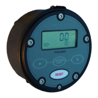
10 Installation
3.3 Wiring connections
Installation 11
3.3 Wiring connections - pulse outputs (for I.S. installations refer to I.S. manual.)
Current Sinking outputs ( NPN )
Current sinking derives its name from the fact that it “sinks current from a load”. The current flows from
the load into the appropriate output (terminal 5).
Driving a logic input The output voltage pulse is typically the internal voltage of the load.
The load w ould normally have an internal pull up resistor on its input.
Driving a coil - - - - - - - The NPN style of output is to be used when driving a coil. The coil load is
obtained by dividing the coil voltage by coil impediance ( Ω ), is expressed in amps & is not to exceed
0.1A. The coil voltage is connected across, & must match, the BT supply voltage & the output (5).
Current Sourcing outputs ( PNP )
Current sourcing gets its name from the fact that it “sources current to a load”. The current flows from the
output (terminal 5) into the load. When w ired as below the output voltage pulse is the supply voltage of
the load. The load w ould normally have an internal pull dow n resistor on its input.
1 + I/P Flow input pulse signal
2 - Vref. Flow input ( coils & voltage type inputs )
3 gnd GND Flow input ( pulse type inputs )
4 +Vdc +Vdc External power , +8~24Vdc (see P14)
5 + ∏ O/P Output pulse ( J1 & J3 selectab le )
6 -gnd GND External power
Wiring practice
Use multi-core screened tw isted pair instrument cable ( 0.5mm
2
) for electrical connection
between the instrument and any remote flow meter or receiving instrument. The screen needs to
be earthed to the signal ground or the receiving instrument, this is to protect the transmitted
signal from mutual inductive interference. Do not earth the screen at both ends of the cable.
Instrument cabling is not be run in a common conduit or parallel w ith power and high inductive
load carrying cables, power surges & power line frequencies may induce erroneous noise
transients onto the signal. Run instrument cables in a dedicated low energy, low voltage conduit.
J1 NPN- PNP selection
J3 Output pulse selection:
F/O non-scaled frequency
P/O scaleable pulse
1 = 1MΩ pull up resistor
2 = 820Ω pull dow n resistor
3 = 0.01µf de-bounce & noise capacitor
( limits max. input freq. to 40hz)
NPN output pulse
( 50mA max.)
pulse output
( 5Khz max.)
pulse output
( 5Khz max.)
PNP output pulse
( 50mA max.)
 Loading...