NINA-B1 series - System Integration Manual
UBX-15026175 - R09 System description
Page 6 of 49
1.1.1 Module architecture
Figure 1: Block diagram of NINA-B1 series
1.1.2 Hardware options
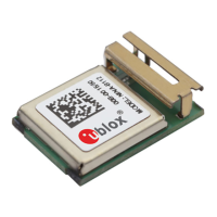
The NINA-B1 series modules use an identical hardware configuration except for the different PCB sizes and
antenna solutions. An on board 32.768 kHz low power crystal is always included and an integrated DC/DC
converter for higher efficiency under heavy load situations.
1.1.3 Software options
The NINA-B1 series module can be used either together with the pre-flashed u-blox connectivity software or as
an Open CPU module where you can run your own application developed with either Arm Mbed, Nordic SDK or
Wirepas development environment inside the NINA-B1 module. The different software options are described in
more detail in section 2.
1.2 Pin configuration and function
1.2.1 Pin attributes
1. FUNCTION: Pin function
2. PIN NAME: The name of the package pin or terminal
3. PIN NUMBER: Package pin numbers associated with each signal
4. POWER: The voltage domain that powers the pin
5. TYPE: Signal type description:
- I = Input
- O = Output
- I/O = Input and Output
- D = Open drain
DC/DC and LDO regulators

 Loading...