SARA-R4 series - System integration manual
UBX-16029218 - R20 Design-in Page 47 of 128
C1-Public
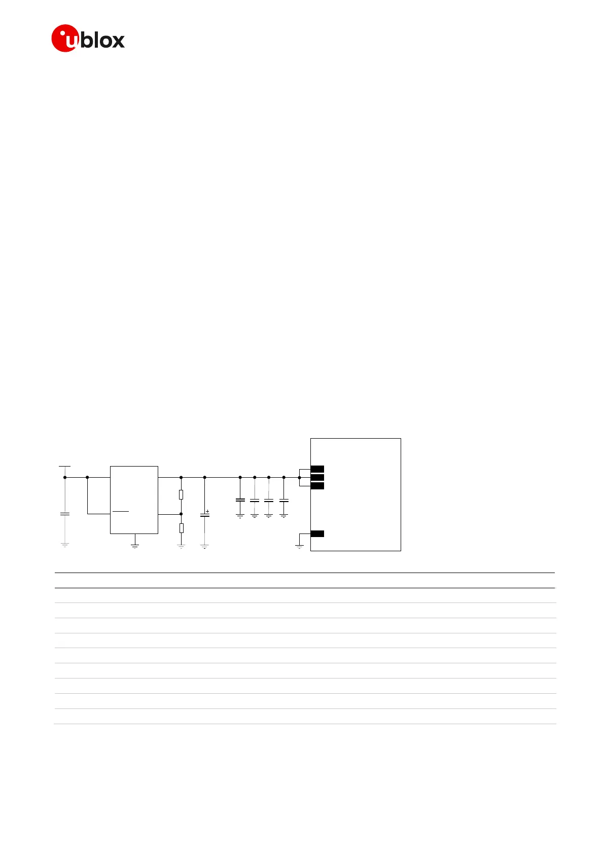
2.2.1.3 Guidelines for VCC supply circuit design using LDO linear regulator
The use of a linear regulator is suggested when the difference from the available supply rail source
and the VCC value is low. The linear regulators provide high efficiency when transforming a 5 VDC
supply to a voltage value within the module VCC normal operating range.
The characteristics of the Low Drop-Out (LDO) linear regulator connected to VCC pins should meet
the following prerequisites to comply with the module VCC requirements summarized in Table 6:
• Power capabilities: the LDO linear regulator with its output circuit must be capable of providing a
voltage value to the VCC pins within the specified operating range and must be capable of
delivering to VCC pins the maximum current consumption occurring during a transmission at the
maximum Tx power, as specified in the SARA-R4 series data sheet [1].
• Power dissipation: the power handling capability of the LDO linear regulator must be checked to
limit its junction temperature to the rated range (i.e. check the voltage drop from the maximum
input voltage to the minimum output voltage to evaluate the power dissipation of the regulator).
Figure 23 and the components listed in Table 13 show an example of a high reliability power supply
circuit for SARA-R4 series modules supporting the 2G radio access technology. This example is also
suitable for the other SARA-R4 series modules, where the VCC module supply is provided by an LDO
linear regulator capable of delivering the highest peak / pulse current specified for the 2G use-case,
with an appropriate power handling capability. The regulator described in this example supports a
wide input voltage range, and it includes internal circuitry for reverse battery protection, current
limiting, thermal limiting and reverse current protection.
It is recommended to configure the LDO linear regulator to generate a voltage supply value slightly
below the maximum limit of the module VCC normal operating range (e.g. ~4.1 V as in the circuit
described in Figure 24 and Table 14). This reduces the power on the linear regulator and improves the
whole thermal design of the supply circuit.
 Loading...


