SARA-R4 series - System integration manual
UBX-16029218 - R20 Design-in Page 90 of 128
C1-Public
2.6.2.2 Guidelines for USB layout design
The USB_D+ / USB_D- lines require accurate layout design to achieve reliable signaling at the high
speed data rate (up to 480 Mb/s) supported by the USB serial interface.
The characteristic impedance of USB_D+ / USB_D- lines is specified by the USB 2.0 specification [6].
The most important parameter is the differential characteristic impedance applicable for the odd-
mode electromagnetic field, which should be as close as possible to 90 differential. Signal integrity
may be degraded if PCB layout is not optimal, especially when the USB signaling lines are very long.
Use the following general routing guidelines to minimize signal quality problems:
• Route USB_D+ / USB_D- lines as a differential pair
• Route USB_D+ / USB_D- lines as short as possible
• Ensure the differential characteristic impedance (Z
0
) is as close as possible to 90
• Ensure the common mode characteristic impedance (Z
CM
) is as close as possible to 30
• Use design rules for USB_D+ / USB_D- as RF transmission lines, being them coupled differential
micro-strip or buried stripline: avoid stubs, abrupt change of layout, and route on clear PCB area
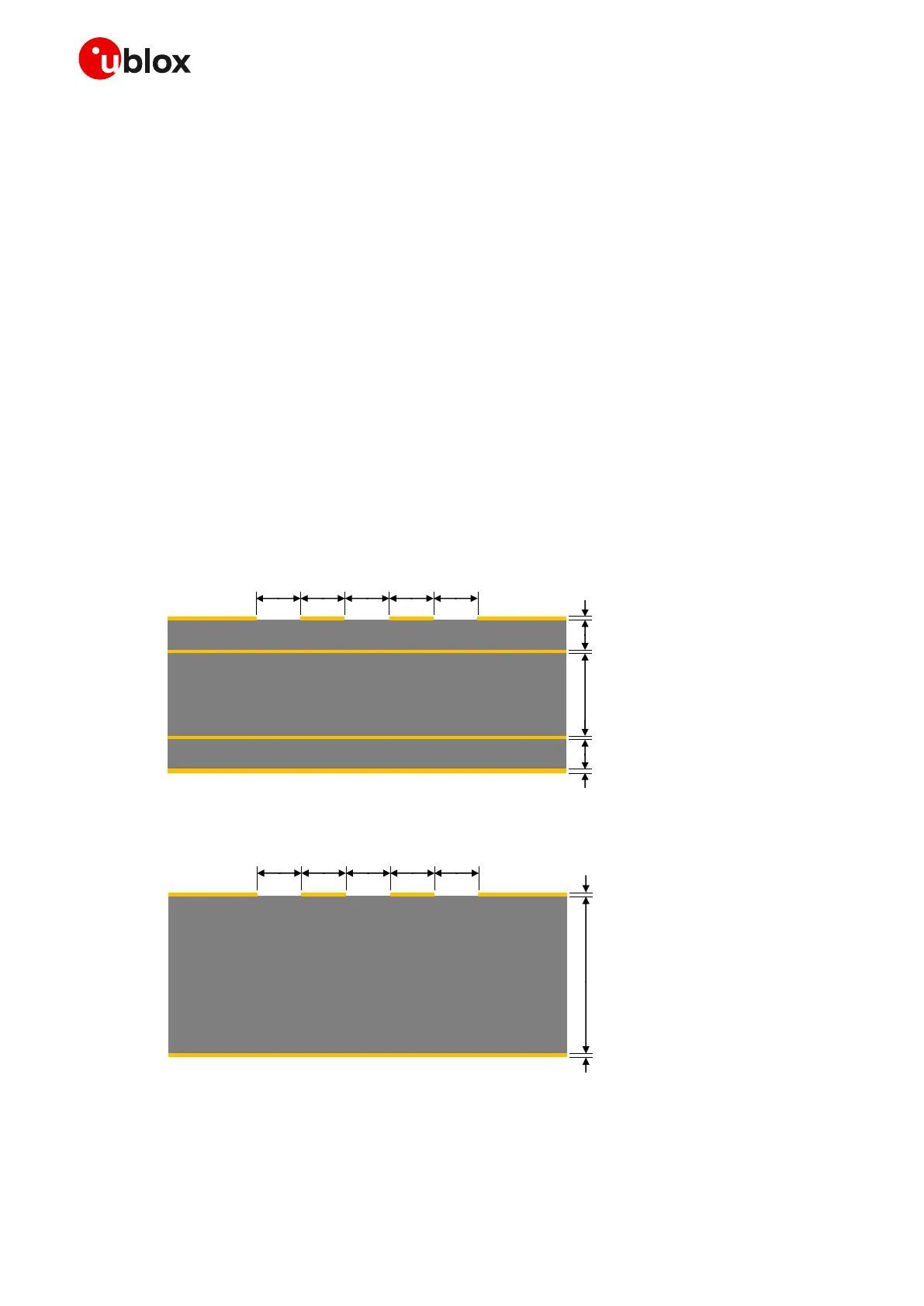
Figure 61 and Figure 62 provide two examples of coplanar waveguide designs with differential
characteristic impedance close to 90 and common mode characteristic impedance close to 30 .
The first transmission line can be implemented in case of 4-layer PCB stack-up herein described, the
second transmission line can be implemented in case of 2-layer PCB stack-up herein described.

 Loading...


