EasyManua.ls Logo

Vertex Standard VX-5500V User Manual

Vertex Standard VX-5500V
80 pages
To Next Page IconTo Next Page
Page #1 background imageLoading...
Page #1 background image
1
Introduction
This manual provides technical information necessary for servicing the VX-5500V VHF FM Transceiver.
Servicing this equipment requires expertise in handling surface-mount chip components. Attempts by non-qualified
persons to service this equipment may result in permanent damage not covered by the warranty, and may be illegal in
some countries.
Two PCB layout diagrams are provided for each double-sided circuit board in the Transceiver. Each side of is referred
to by the type of the majority of components installed on that side (“leaded” or “chip-only”). In most cases one side has
only chip components, and the other has either a mixture of both chip and leaded components (trimmers, coils, electrolyt-
ic capacitors, ICs, etc.), or leaded components only.
While we believe the technical information in this manual to be correct, VERTEX STANDARD assumes no liability
for damage that may occur as a result of typographical or other errors that may be present. Your cooperation in pointing
out any inconsistencies in the technical information would be appreciated.
©2003 VERTEX STANDARD CO., LTD. EC034N90A
Service Manual
VX-5500V
VHF FM Transceiver
Operating Manual Reprint ......................... 1-1
Cloning ....................................................................
2-1
Specifications ................................................ 2-2
Exploded View & Miscellaneous Parts ... 3-1
Block Diagram .............................................. 3-2
Interconnection Diagram ............................ 3-4
Circuit Description...................................... 4-1
Alignment ...................................................... 5-1
Contents
Board Unit (
Schematics, Layouts & Parts
)
MAIN Unit........................................................... 6A-1
DISPLAY Unit ...................................................... 6B-1
KEY Unit ............................................................... 6C-1
VR Unit ................................................................. 6D-1
MIC CONN Unit................................................. 6D-2
Optional Board Unit (
Schematics, Layouts & Parts
)
F2D-8 2-Tone Decode Unit ................................ 7A-1
VTP-50 VX-Trunk Unit ....................................... 7B-1
FVP-25 Encryption / DTMF Pager Unit ............7C-1
F5D-14 5-Tone Unit ............................................ 7D-1
FIF-7A Connection Unit...................................... 7E-1
POWE R
VERTEX STANDARD CO., LTD.
4-8-8 Nakameguro, Meguro-Ku, Tokyo 153-8644, Japan
VERTEX STANDARD
US Headquarters
10900 Walker Street, Cypress, CA 90630, U.S.A.
International Division
8350 N.W. 52nd Terrace, Suite 201, Miami, FL 33166, U.S.A.
YAESU EUROPE B.V.
P.O. Box 75525, 1118 ZN Schiphol, The Netherlands
YAESU UK LTD.
Unit 12, Sun Valley Business Park, Winnall Close
Winchester, Hampshire, SO23 0LB, U.K.
VERTEX STANDARD HK LTD.
Unit 5, 20/F., Seaview Centre, 139-141 Hoi Bun Road,
Kwun Tong, Kowloon, Hong Kong

Other manuals for Vertex Standard VX-5500V

Question and Answer IconNeed help?

Do you have a question about the Vertex Standard VX-5500V and is the answer not in the manual?

Vertex Standard VX-5500V Specifications

General IconGeneral
BrandVertex Standard
ModelVX-5500V
CategoryTransceiver
LanguageEnglish

Summary

Service Manual Introduction

Controls and Connectors Overview

Front Panel Controls and Display

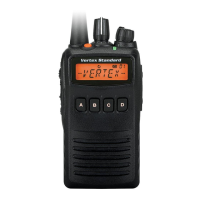
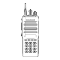
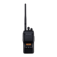
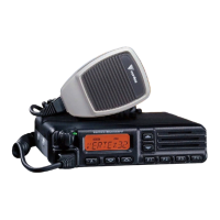
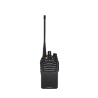
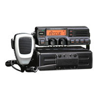
Details the front panel buttons, indicators, and display of the transceiver.

Side and Rear Panel Connectors

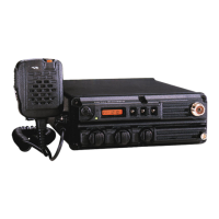
Describes the microphone jack, external speaker, DC power, and accessory connectors.

Basic Transceiver Operation

Powering On/Off and Volume Adjustment

Instructions for turning the transceiver on/off and adjusting audio volume levels.

Transmitting and Channel Selection

Procedures for transmitting and selecting operating channels or groups.

Advanced Transceiver Operation

Programmable Function (PF) Buttons

Explains customizable PF button functions and their assignments.

Channel Scan and Dual Watch Features

Details on activating and using channel scanning and dual watch functions.

ARTS and PF Button Functions Overview

Description of Auto Range Transpond System and general PF button usage.

Specific PF Button Functions (Part 1)

Explains functions like DIM, EMG, HA, Home Channel, Intercom, and Low Power.

Specific PF Button Functions (Part 2)

Covers GRP/CH UP/DWN, AUX, PA, MONI, RCL, ST, SP, SQL functions.

Compander and Encryption (Option) Functions

Details the Compander IC function and optional Encryption feature.

Optional Accessories and Parts

DSUB 25-Pin Accessory Connector Details

DSUB 25-Pin: RSSI [Analog Output]

Describes the RSSI analog output pin and its signal strength graph.

DSUB 25-Pin: Programmable Input Ports (Pins 2-6)

Details programmable input port features and example assignments.

DSUB 25-Pin: Universal Input Port and Data/Control Pins (Pins 7-12)

Explains channel recall, data I/O, transmit, and mute pins.

DSUB 25-Pin: Power, Ignition, and Output Pins (Pins 13-25)

Data, power, ignition sense, output, squelch, and mute pins.

Radio Cloning Procedure

Radio Cloning Steps

Step-by-step guide for transferring programming data between transceivers.

Dealer Programming for Optional Boards

Procedure for programming optional VTP-50 and F5D-14 boards.

Transceiver Specifications

General Transceiver Specifications

Covers number of channels, frequency range, power, dimensions, and weight.

Receiver and Transmitter Performance Specs

Detailed technical performance metrics for receiver and transmitter sections.

Exploded View and Parts Identification

Screw and Accessories List

Lists screws, fuses, cables, knobs, and nameplates used in assembly.

Exploded View Assembly Diagram

Visual breakdown of the transceiver's main assembly and components.

Main Unit Block Diagram

Panel Block Diagram

Interconnection Diagram Details

Interconnection Diagram: Unit Connections and Pinouts

Illustrates how units connect and details pin functions for various connectors.

Circuit Description - Receiver and PLL Synthesizer

Circuit Description: Receiver Signal Path

Explains the RF signal flow from antenna to audio output via IF stages.

Circuit Description: PLL Synthesizer Operation

Details the PLL synthesizer's role in frequency generation and modulation.

Circuit Description - Transmitter, Demodulator, MPU, EEPROM

Circuit Description: Transmitter Path and Modulation

Describes audio processing, FM modulation, RF power output, and harmonic suppression.

Circuit Description: Demodulators, MPU, and EEPROM

Explains DCS/CTCSS demodulation, MPU control, and EEPROM data storage.

Transceiver Alignment Procedures

Alignment: Required Test Equipment and Precautions

Lists necessary test gear and crucial preparation steps for realignment.

Alignment: Preparation and Thermal Considerations

Details environmental and setup requirements for accurate alignment.

Alignment: EEPROM Data and PLL/Transmitter Steps

Downloading EEPROM data and aligning PLL/transmitter parameters.

Alignment: PLL VCV and Reference Frequency

Adjusting PLL VCV and confirming reference frequency for stability.

Alignment: Transmitter Power and Deviation

Steps to set transmitter output power and adjust max deviation levels.

Alignment: CTCSS and DCS Modulation Levels

Adjusting deviation levels for CTCSS and DCS modulation.

Alignment: Receiver Alignment and SINAD

Procedure for receiver tuning to achieve optimal SINAD levels.

Alignment: Squelch Threshold Adjustment

Adjusting squelch threshold levels for Wide and Narrow band reception.

Board Unit Schematics, Layouts, and Parts

Main Unit Schematics, Layout, and Parts

Detailed diagrams and parts list for the main transceiver unit.

Display Unit Schematics, Layout, and Parts

Diagrams and parts list for the display and control interface unit.

Key Unit Schematics, Layout, and Parts

Schematics, layout, and parts for the key input unit.

VR Unit Schematics, Layout, and Parts

Diagrams and parts list for the Volume/Rotary control unit.

MIC CONN Unit Schematics, Layout, and Parts

Schematics, layout, and parts for the microphone connection unit.

Optional Board Unit Schematics, Layouts, and Parts

F2D-8 2-Tone Decode Unit Schematics and Parts

Schematics and parts list for the 2-Tone Decode Unit.

VTP-50 VX-Trunk Unit Schematics and Parts

Schematics and parts list for the VX-Trunk Unit.

FVP-25 Encryption/DTMF Pager Unit Schematics and Parts

Schematics and parts list for the Encryption/DTMF Pager Unit.

F5D-14 5-Tone Unit Schematics and Parts

Schematics and parts list for the 5-Tone Unit.

FIF-7A Connection Unit Schematics and Parts

Schematics and parts list for the FIF-7A Connection Unit.

Related product manuals