ViewSonic Corporation
Confidential - Do Not Copy VP2650wb-1
23
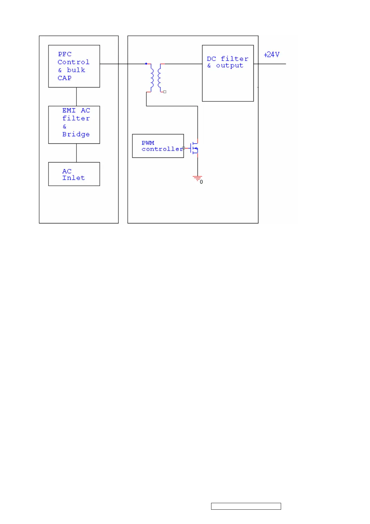
A-2.) Power board diagram:
The power board have two function blocks , one is power factor correction ( PFC ), the other
one is PWM to get DC output .
A-3.) PFC circuit introduction :
IC651( L6562) is a preregulator for power factor correction . The function and circuit is similar
to step-up stage.
It can boost low AC input voltage to bulk capacitor to get higher power factor.
Pin 1. is the inverting input of the error amplifier. R671,R672,R673,R674 are resistive divider
and are connected brtween the output regulated voltage and this point , to provide voltage
feedback.
Pin 2. is the output of amplifier. A feedback compensation network is placed between this pin
and the Pin 1.
Pin 3. is the input of the multiplier stage. R657,R658,R659 are resistive divider and are
connected to this pin the rectified mains . A voltage signal , proportional to the rectifed mains ,
appears on this pin .
Pin 4. is the input to the comparator of the control loop . The current is sensed by resistor
R670 and the resulting voltage is applied to this pin .
Pin 5. is the zero current detection input . If it is connected to GND , the device will be
disabled.
Pin 6. is the current return for driver and control circuits .
Pin 7. is the gate driver output . A push pull output stage is able to drive the power MOS .
Pin 8. is supply voltage of driver and control circuits.

 Loading...