WM_PRJ_Q2400_PTS_005 -007
18th January 2006
Confidential©
All rights reserved
Page: 23 / 51
This document is the sole and exclusive property of WAVECOM. Not to be
distributed or divulged without prior written agreement.
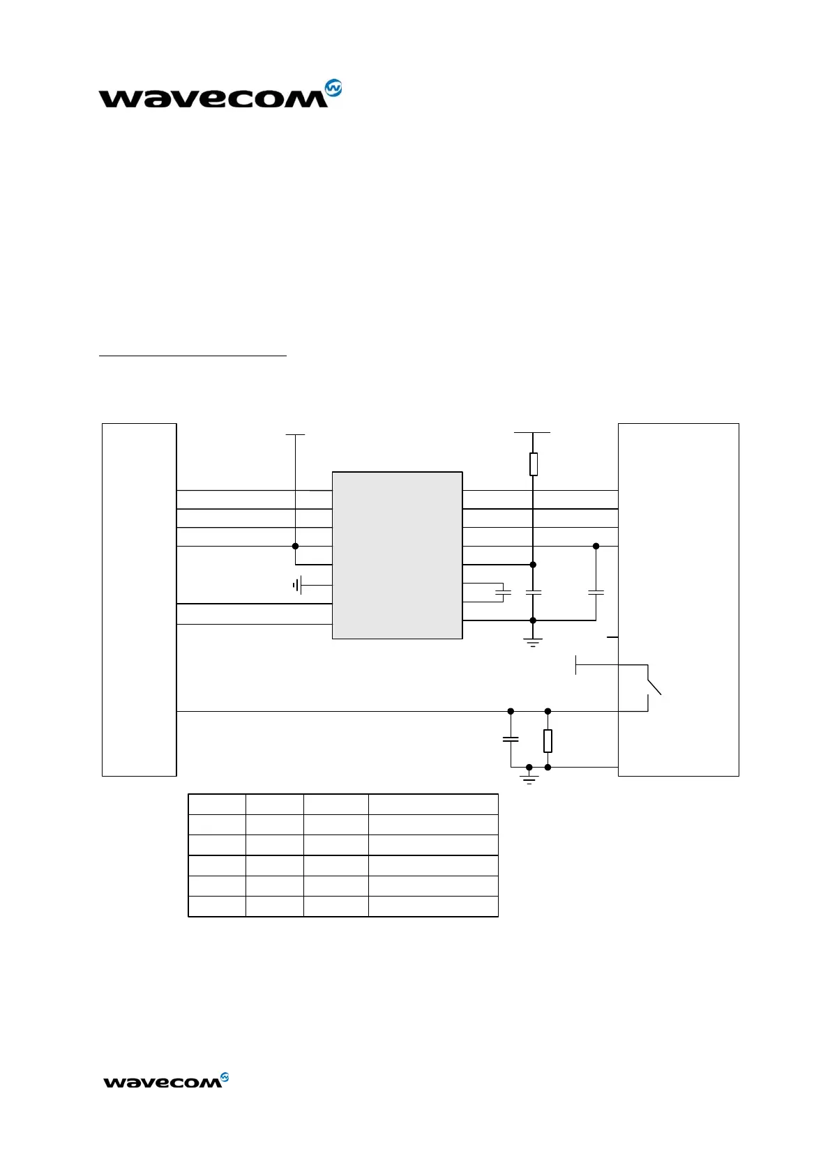
2.2.6.3 SIM 3 V / 5 V management
It is possible to manage 3 V and 5 V SIM cards using an external level shifter
device (see Figure below).
In this case, depending on the type of SIM detected, the module firmware
triggers the GPO0 output signal (pin #26) in order to properly set the external
SIM driver level (3 V or 5 V).
As for 3 V SIM, it is recommended to add Transient Voltage Suppressors on the
signals connected to the SIM socket (refer to Figure 10).
Typical implementation:
CIN
RIN
DATA
DDRV
DVCC
M2
M1
M0
CLK
RST
I/O
VCC
VIN
C1+
C1-
GND
LTC1555L-1.8
1
2
3
4
5
6
7
8
16
15
14
13
12
11
10
9
VCC
2.8 V
WISMO
Q2400
SIM_CLK
SIM_RST
SIM_DATA
GPO0
SIM_VCC
SIM
Socket
VCC
2.8 V
2.2 µF
100 nF
LEVEL SHIFTER
3
CLK
2
RST
7
I/O
1
VCC = 3 V or 5 V
IVCC = 10 mA
6
VPP
VCC
4
CC4
8
CC8
1 µF
SIM_PRES
5
GND
470 pF
100 kΩ
VCC
1 Ω
to
4.7 Ω
DVCC = 2.8 V
Operating Mode
Truth
table:
M0
0V
0V
DVCC
DVCC
DVCC
M1
0V
0V
0V
DVCC
DVCC
M2
DVCC
0V
0V or DVCC
0V or DVCC
0V or DVCC
Shutdown (VCC = 0V)
VCC = VIN
VCC = 3 V
VCC = 1.8 V
VCC = 5 V
Figure 10: Example of 3 V / 5 V SIM interface implementation
 Loading...