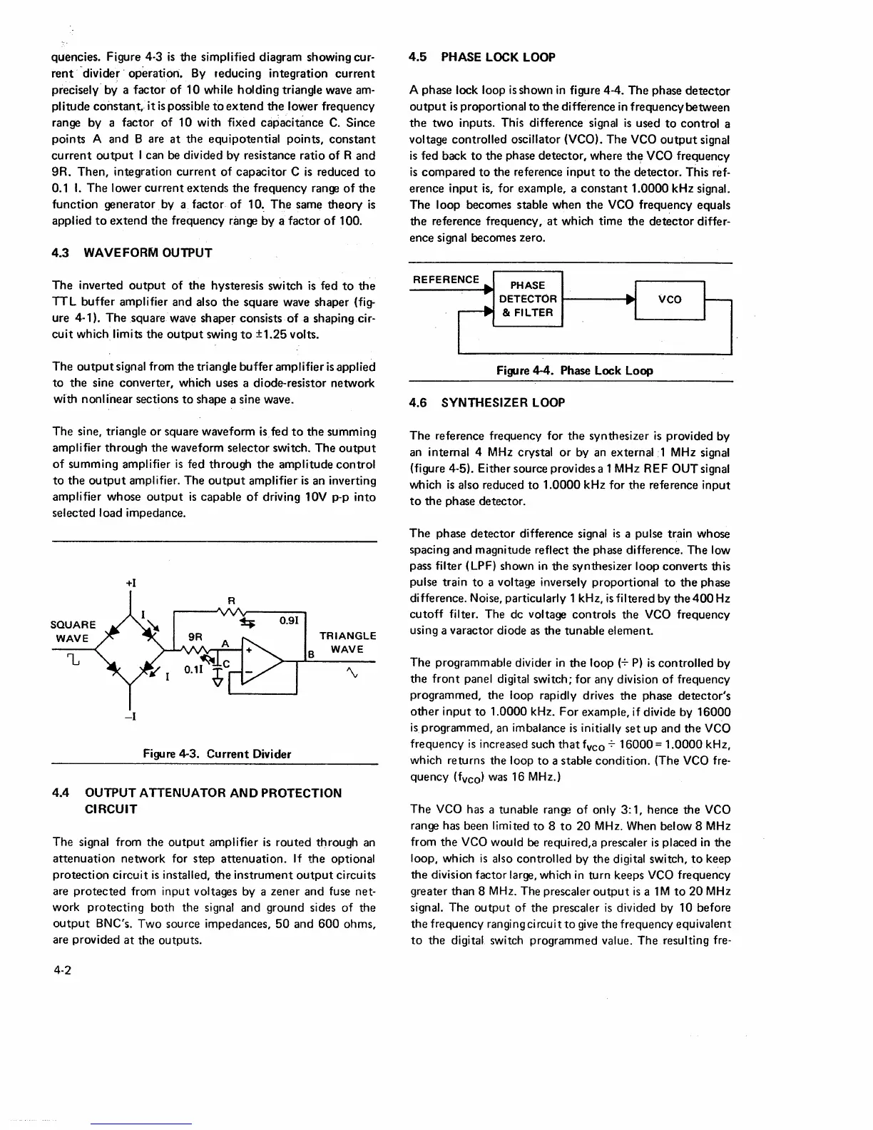
quencies. Figure 4-3
is
the simplified diagram showing cur-
rent
-divider· operation.
By
reducing integration
current
precisely. by a factor
of
10
while holding triangle wave am-
plitude
constant,
it
is
possible
to
extend
the
lower frequency
range by a factor
of
10 with fixed capacitance
C.
Since
points
A and 8 are
at
the equipotential points,
constant
current
output
I can be divided by resistance ratio
of
R and
9R.
Then,
integration
current
of
capacitor
C
is
reduced
to
0.1 I.
The
lower
current
extends
the
frequency range
of
the
function generator by a factor
of
1
O~
The
same
theory
is
applied
to
extend
the
frequency range by a factor
of
100.
4.3 WAVEFORM OUTPUT
The
inverted
output
of
the
hysteresis switch
is
fed
to
the
TTL
buffer
amplifier and also
the
square wave shaper (fig-
ure 4-1
).
The
square wave shaper consists.
of
a shaping cir-
cuit
which limits the
output
swing
to
±1.25 volts.
The
output
signal from the triangle
buffer
amplifier
is
applied
to
the
sine converter, which uses a diode-resistor network
with nonlinear sections
to
shape a sine wave.
The
sine, triangle
or
square waveform
isfed
to
the
summing
amplifier through the waveform selector switch.
The
output
of
summing amplifier
is
fed through
the
amplitude
control
to
the
output
amplifier. The
output
amplifier
is
an inverting
amplifier whose
output
is
capable
of
driving 10V p-p
into
selected load impedance.
SQUARE
WAVE
+I
-I
Figure 4-3.
Current
Divider
TRIANGLE
B
WAVE
4.4 OUTPUT ATTENUATOR
AND
PROTECTION
CIRCUIT
The signal from the
output
amplifier
is
routed
through an
attenuation
network for step
attenuation.
If
the
optional
protection
circuit
is
installed, the
instrument
output
circuits
are
protected
from input voltages by a zener and fuse net-
work
protecting
both the signal and ground sides
of
the
output
BNC's. Two source impedances,
50
and
600
ohms,
are provided
at
the outputs.
4-2
4.5 PHASE LOCK
LOOP
A phase lock loop
is
shown
in
figure 4-4. The phase
detector
output
is
proportional
to
the
difference in frequency between
the
two
inputs. This difference signal
is
used
to
control a
voltage controlled oscillator (VCO). The VCO
output
signal
is
fed back
to
the
phase
detector,
where
th~
VCO frequency
is
compared
to
the reference
input
to
the detector. This ref-
erence
input
is,
for example, a
constant
1.0000
kHz signal.
The loop becomes stable when
the
VCO
frequency equals
the reference frequency,
at
which time
the
detector
differ-
ence signal becomes zero.
REFERENCE
PHASE
DETECTOR
~----
&FILTER
Figure 4-4. Phase
lock
loop
4.6 SYNTHESIZER LOOP
VCO
The reference frequency for
the
synthesizer
is
provided by
an internal 4
MHz
crystal
or
by an external 1
MHz
signal
(figure 4-5). Either source provides a 1 MHz REF OUT signal
which
is
also reduced
to
1.0000
kHz for the reference
input
to
the
phase detector.
The
phase
detector
difference signal
is
a pulse train whose
spacing and magnitude reflect
the
phase difference. The low
pass filter ( LPF) shown in
the
synthesizer loop converts this
pulse train
to
a voltage inversely proportional
to
the
phase
difference. Noise, particularly 1 kHz,
is
filtered by the
400
Hz
cutoff
filter. The de voltage controls the VCO frequency
using a varactor diode
as
the
tunable element.
The programmable divider
in
the
loop (7
P)
is
controlled by
the
front
panel digital switch; for any division
of
frequency
programmed, the loop rapidly drives the phase
detector's
other
input
to
1.0000 kHz.
For
example, if divide by
16000
is
programmed, an imbalance
is
initially
set
up
and
the
VCO
frequency
is
increased such
that
f
vco-=-
16000
=
1.0000
kHz,
which returns the loop
to
a stable condition. (The
VCO
fre-
quency (fvco) was 16 MHz.)
The
VCO has a tunable range
of
only 3:
1,
hence
the
VCO
range has been limited
to
8
to
20
MHz. When below 8
MHz
from
the
VCO would be required,a prescaler
is
placed
in
the
loop, which
is
also controlled by
the
digital switch,
to
keep
the
division factor large, which
in
turn keeps VCO frequency
greater than
8
MHz.
The prescaler
output
is
a 1 M
to
20
MHz
signal. The
output
of the prescaler
is
divided by
10
before
the
frequency
rangingcircuitto
give
the frequency equivalent
to
the
digital switch programmed value. The resulting fre-
 Loading...