Memory 103
Xilinx Blocks
by the port’s address input. During a write cycle, the user can configure the behavior
of the data out ports A/B to one of the following choices:
• Read After Write
• Read Before Write
• No Read On Write
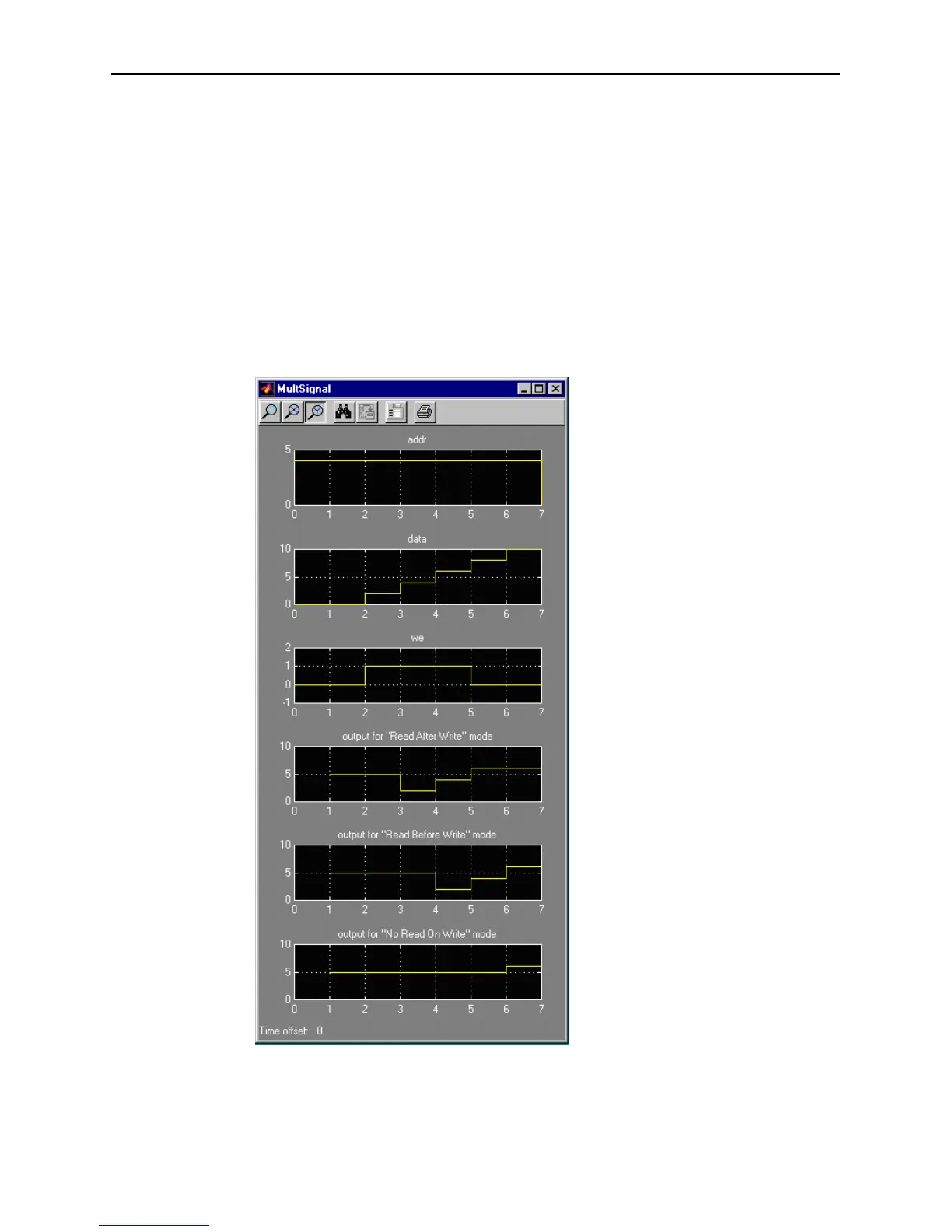
The write modes can be described with the help of the figure below. In the figure, the
memory has been set to an initial value of 5 and the address bit is specified as 4. When
using No Read On Write mode, the output is unaffected by the address line and the
output is the same as the last output when the WE was 0. For the other two modes, the
output is obtained from the location specified by the address line, and hence is the
value of the location being written to. This means that the output can be the old value
which corresponds to Read After Write.
Figure 3-70: Illustration of write modes