EasyManua.ls Logo

Xilinx XC4000 Series User Manual

Xilinx XC4000 Series
55 pages
To Next Page IconTo Next Page
To Previous Page IconTo Previous Page
Page #26 background imageLoading...
Page #26 background image
XC4000 Series Field Programmable Gate Arrays
4-30 September 18, 1996 (Version 1.04)
The buffer enable is an active-High 3-state (i.e. an active-
Low enable), as shown in Table 15.
Another 3-state buffer with similar access is located near
each I/O block along the right and left edges of the array.
(See Figure 33 on page 39.)
The horizontal longlines driven by the 3-state buffers have a
weak keeper at each end. This circuit prevents undefined
floating levels. However, it is overridden by any driver, even
a pull-up resistor.
Special longlines running along the perimeter of the array
can be used to wire-AND signals coming from nearby IOBs
or from internal longlines. These longlines form the wide
edge decoders discussed in “Wide Edge Decoders” on
page 31.
Three-State Buffer Modes
The 3-state buffers can be configured in three modes:
Standard 3-state buffer
Wired-AND with input on the I pin
Wired OR-AND
Standard 3-State Buffer
All three pins are used. Place the library element BUFT.
Connect the input to the I pin and the output to the O pin.
The T pin is an active-High 3-state (i.e. an active-Low
enable). Tie the T pin to Ground to implement a standard
buffer.
Wired-AND with Input on the I Pin
The buffer can be used as a Wired-AND. Use the WAND1
library symbol, which is essentially an open-drain buffer.
WAND4, WAND8, and WAND16 are also available. See
the
XACT Libraries Guide
for further information.
The T pin is internally tied to the I pin. Connect the input to
the I pin and the output to the O pin. Connect the outputs of
all the WAND1s together and attach a PULLUP symbol.
Wired OR-AND
The buffer can be configured as a Wired OR-AND. A High
level on either input turns off the output. Use the
WOR2AND library symbol, which is essentially an open-
drain 2-input OR gate. The two input pins are functionally
equivalent. Attach the two inputs to the I0 and I1 pins and
tie the output to the O pin. Tie the outputs of all the
WOR2ANDs together and attach a PULLUP symbol.
Three-State Buffer Examples
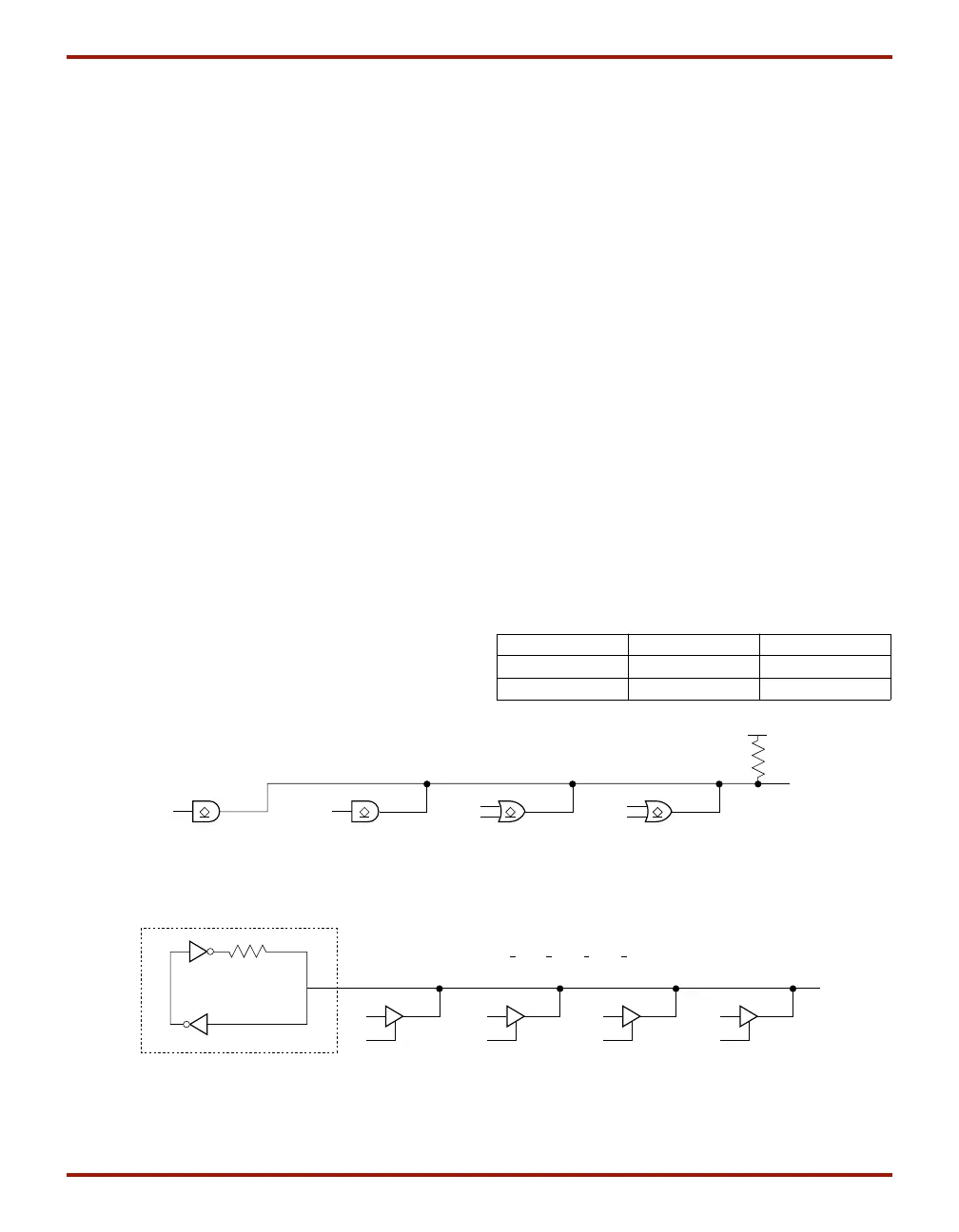
Figure 22 shows how to use the 3-state buffers to imple-
ment a wired-AND function. When all the buffer inputs are
High, the pull-up resistor(s) provide the High output.
Figure 23 shows how to use the 3-state buffers to imple-
ment a multiplexer. The selection is accomplished by the
buffer 3-state signal.
Pay particular attention to the polarity of the T pin when
using these buffers in a design. Active-High 3-state (T) is
identical to an active-Low output enable, as shown in
Table 15.
Table 15: Three-State Buffer Functionality
IN T OUT
X1Z
IN0IN
P
U
L
L
U
P
Z = D
A
D
B
(D
C
+D
D
) (D
E
+D
F
)
D
E
D
F
D
C
D
D
D
B
D
A
WAND1 WAND1
W0R2AND W0R2AND
X6465
Figure 22: Open-Drain Buffers Implement a Wired-AND Function
D
N
D
C
D
B
D
A
ABCN
Z = D
A
• A + D
B
• B + D
C
• C + D
N
• N
~100 k
"Weak Keeper"
X6466
BUFT BUFT BUFT BUFT
Figure 23: 3-State Buffers Implement a Multiplexer

Table of Contents

Question and Answer IconNeed help?

Do you have a question about the Xilinx XC4000 Series and is the answer not in the manual?

Xilinx XC4000 Series Specifications

General IconGeneral
FamilyXC4000
CategoryFPGA
TechnologyCMOS
Supply Voltage5V
Operating Voltage5V
Package OptionsPGA, PQFP
Package TypesPGA, PQFP

Summary

XC4000-Series Features

Additional XC4000EX/XL Features

Details specific enhancements for XC4000EX/XL families, including higher capacity and routing.

Low-Voltage Versions Available

Information on low-voltage XC4000L and XC4000XL device variants.

Introduction

Overview of XC4000-Series FPGAs, their benefits, and history.

Description

General description of the XC4000-Series architecture, software support, and applications.

Taking Advantage of Reconfiguration

XC4000E and XC4000EX Families Compared to the XC4000

Increased System Speed

Discusses performance improvements in XC4000E/EX over older families, citing MHz rates.

PCI Compliance

States that XC4000-Series -3 and faster speed grades are PCI compliant.

Carry Logic

Details the significantly faster carry logic chain in XC4000-Series devices.

Select-RAM Memory: Edge-Triggered, Synchronous RAM Modes

Describes the on-chip RAM configuration options for synchronous and edge-triggered writes.

Dual-Port RAM

Explains the dual-port RAM option for 16x1 configurations within CLBs.

IOB Clock Enable

Covers the common clock enable input for IOB flip-flops, enhancing versatility.

Input Thresholds

Discusses globally configurable input thresholds for TTL and CMOS levels.

Global Signal Access to Logic

Configuration Pin Pull-Up Resistors

Soft Start-up

XC4000 and XC4000A Compatibility

Additional Improvements in XC4000EX Only

Increased Routing

Highlights additional vertical and horizontal interconnect lines in the XC4000EX.

Faster Input and Output

Covers dedicated early clock buffers for fast input data capture and output.

Latch Capability in CLBs

Notes the ability to configure CLB storage elements as latches in XC4000EX.

IOB Output MUX From Output Clock

Describes the IOB output multiplexer for pad sharing or 2-input function generation.

Express Configuration Mode

Introduces a new slave configuration mode accepting parallel data input for faster rates.

Additional Address Bits

Mentions extended addressing in Master Parallel configuration mode for larger devices.

Detailed Functional Description

Basic Building Blocks

Introduces CLBs, IOBs, TBUFs, wide edge decoders, and an on-chip oscillator.

Configurable Logic Blocks (CLBs)

The core logic elements providing programmable functionality.

Flip-Flops

Explains the two D-type flip-flops in CLBs with common clock and enable inputs.

Latches (XC4000EX only)

Describes the optional latch configuration for CLB storage elements in XC4000EX.

Clock Input

Details the common clock pin K for CLB flip-flops, with independent invertibility.

Clock Enable

Explains the active-High clock enable signal (EC) shared by CLB storage elements.

Set/Reset

Covers the asynchronous storage element input (SR) for set or reset configuration.

Global Set/Reset

Describes the dedicated global set/reset net (GSR) for synchronous reset of storage elements.

Data Inputs and Outputs

Details how storage element data inputs are driven and CLB outputs are generated.

Control Signals

Explains how control inputs map to internal signals like EC, SR/H0, DIN/H2, and H1.

Using FPGA Flip-Flops and Latches

Discusses using CLB flip-flops for pipelined designs to increase performance.

Using Function Generators as RAM

RAM Configuration Options

Lists RAM array sizes (16x2, 32x1, 16x1) and timing modes (edge-triggered, level-sensitive).

Choosing a RAM Configuration Mode

Guides selection of RAM mode based on timing, resources, and design simplicity.

Detailed Functional Description

Configurable Logic Blocks (CLBs)

The core logic elements providing programmable functionality.

RAM Inputs and Outputs

Details how CLB pins function as address, data, and control lines for RAM configurations.

Single-Port Edge-Triggered Mode

Explains the timing and operation of edge-triggered single-port RAM, similar to data registers.

Dual-Port Edge-Triggered Mode

Describes dual-port RAM operation for simultaneous read/write at two addresses.

Single-Port Level-Sensitive Timing Mode

Initializing RAM at Configuration

Explains how RAM contents are initialized during device configuration, defaulting to zeros.

Fast Carry Logic

Input/Output Blocks (IOBs)

IOB Input Signals

Covers input paths, registers (flip-flop/latch), and global configuration of input thresholds.

Registered Inputs

Explains input register behavior, including clock enable and storage element modes.

IOB Output Signals

Details output buffer configurations, including slew rate, pull-up/down, and 3-state control.

Optional Delay Guarantees Zero Hold Time

Discusses optional delay elements in IOBs to ensure zero hold time for inputs.

Additional Input Latch for Fast Capture (XC4000EX only)

Describes an optional latch in XC4000EX IOBs for fast input data capture synchronized to internal clocks.

Output Multiplexer/2-Input Function Generator (XC4000EX only)

Details the XC4000EX IOB output multiplexer for pad sharing or 2-input function generation.

Other IOB Options

Pull-up and Pull-down Resistors

Explains the use of programmable pull-up and pull-down resistors for unused pins.

Independent Clocks

Mentions separate clock signals for IOB input and output flip-flops, with independent inversion.

Early Clock for IOBs (XC4000EX only)

Covers special early clocks sourced by global buffers for faster IOB access.

Fast Clock for IOBs (XC4000EX only)

Details very fast clocks driven by FastCLK buffers for minimal setup and clock-to-out times.

Global Set/Reset

Describes the use of the Global Set/Reset signal (GSR) for IOB registers.

JTAG Support

Mentions embedded logic for IEEE 1149.1 boundary scan testing.

Three-State Buffers

Explains buffers associated with CLBs for driving longlines and implementing buses.

Wide Edge Decoders

On-Chip Oscillator

Details the internal oscillator running at approximately 8 MHz for configuration and timing.

Programmable Interconnect

Interconnect Overview

Describes the types of interconnect: CLB routing, IOB routing (VersaRing), and Global routing.

CLB Routing Connections

Details the routing resources associated with CLBs, including PSMs and line types.

Programmable Switch Matrices

Explains switch matrices (PSMs) that establish connections between interconnect lines.

Single-Length Lines

Discusses single-length lines offering flexibility and fast routing between adjacent blocks.

Double-Length Lines

Describes double-length lines providing faster routing over intermediate distances.

Quad Lines (XC4000EX only)

Longlines

Direct Interconnect (XC4000EX only)

I/O Routing

Octal I/O Routing (XC4000EX only)

Global Nets and Buffers

Global Nets and Buffers (XC4000E only)

Explains dedicated global networks and buffers for clock distribution in XC4000E devices.

Global Nets and Buffers (XC4000EX only)

Details global nets and buffers specific to XC4000EX devices, including clock buffer options.

Choosing an XC4000EX Clock Buffer

Guides the selection of clock buffers (BUFGLS, BUFGE, BUFFCLK) for XC4000EX designs.

Global Low-Skew Buffers

Describes standard clock buffers (BUFGLS) for driving most of the device with minimal skew.

Global Early Buffers

Details BUFGE for faster clock access with limited CLB reach, aiding I/O interface.

FastCLK Buffers

Explains BUFFCLK for the fastest possible I/O clock path into the XC4000EX.

Power Distribution

Pin Descriptions

User I/O Pins That Can Have Special Functions

Lists I/O pins that can be configured for special functions like RDY/BUSY, RCLK, and mode pins.

Boundary Scan

Data Registers

Explains the boundary scan register and other data registers, including BSCANT.UPD.

Instruction Set

Covers the XC4000-Series boundary scan instruction set for device configuration and data access.

Bit Sequence

Describes the bit sequence within each IOB for boundary scan data registers.

Including Boundary Scan in a Schematic

Details how to include boundary scan schematic elements for configuration or continuous use.

Avoiding Inadvertent Boundary Scan Activation

Provides methods to prevent unintentional boundary scan activation during configuration.

Product Availability

User I/O Per Package

Lists maximum available user I/O counts per device and package combination.

Ordering Information

Related product manuals