September 18, 1996 (Version 1.04) 4-53
Bit Sequence
The bit sequence within each IOB is: In, Out, 3-State. The
input-only M0 and M2 mode pins contribute only the In bit
to the boundary scan I/O data register, while the output-
only M1 pin contributes all three bits.
The first two bits in the I/O data register are TDO.T and
TDO.O, which can be used for the capture of internal sig-
nals. The final bit is BSCANT.UPD, which can be used to
drive an internal net. These locations are primarily used by
Xilinx for internal testing.
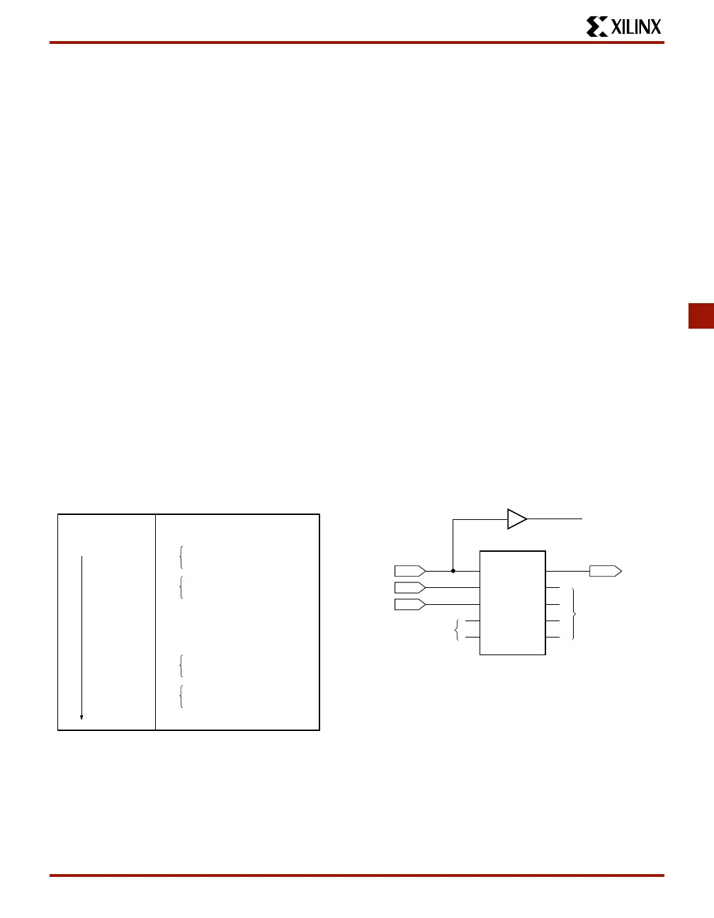
From a cavity-up view of the chip (as shown in XDE or
Epic), starting in the upper right chip corner, the boundary
scan data-register bits are ordered as shown in Figure 44.
The device-specific pinout tables for the XC4000 Series
include the boundary scan locations for each IOB pin.
BSDL (Boundary Scan Description Language) files for
XC4000-Series devices are available on the Xilinx BBS.
Including Boundary Scan in a Schematic
If boundary scan is only to be used during configuration, no
special schematic elements need be included in the sche-
matic or HDL code. In this case, the special boundary scan
pins TDI, TMS, TCK and TDO can be used for user func-
tions after configuration.
To indicate that boundary scan remain enabled after config-
uration, place the BSCAN library symbol and connect the
TDI, TMS, TCK and TDO pad symbols to the appropriate
pins, as shown in Figure 45.
Even if the boundary scan symbol is used in a schematic,
the input pins TMS, TCK, and TDI can still be used as
inputs to be routed to internal logic. Care must be taken not
to force the chip into an undesired boundary scan state by
inadvertently applying boundary scan input patterns to
these pins. The simplest way to prevent this is to keep TMS
High, and then apply whatever signal is desired to TDI and
TCK.
Avoiding Inadvertent Boundary Scan
Activation
If TMS or TCK is used as user I/O, care must be taken to
ensure that at least one of these pins is held constant dur-
ing configuration. In some applications, a situation may
occur where TMS or TCK is driven during configuration.
This may cause the device to go into boundary scan mode
and disrupt the configuration process.
To prevent activation of boundary scan during configura-
tion, do either of the following:
• TMS: Tie High to put the Test Access Port controller
in a benign RESET state
• TCK: Tie High or Low—don't toggle this clock input.
For more information regarding boundary scan, refer to the
Xilinx Application Note XAPP 017.001, “
Boundary Scan in
XC4000E Devices
.“
Bit 0 ( TDO end)
Bit 1
Bit 2
TDO.T
TDO.O
Top-edge IOBs (Right to Left)
Left-edge IOBs (Top to Bottom)
MD1.T
MD1.O
MD1.I
MD0.I
MD2.I
Bottom-edge IOBs (Left to Right)
Right-edge IOBs (Bottom to Top)
B SCANT.UPD
(TDI end)
X6075
Figure 44: Boundary Scan Bit Sequence
TDI
TMS
TCK
TDO1
TDO2
TDO
DRCK
IDLE
SEL1
SEL2
TDI
TMS
TCK
TDO
BSCAN
To User
Logic
IBUF
Optional
From
User Logic
To User
Logic
X2675
Figure 45: Boundary Scan Schematic Example
 Loading...