XC4000 Series Field Programmable Gate Arrays
4-12 September 18, 1996 (Version 1.04)
Implementing wide functions in a single block reduces both
the number of blocks required and the delay in the signal
path, achieving both increased capacity and speed.
The versatility of the CLB function generators significantly
improves system speed. In addition, the design-software
tools can deal with each function generator independently.
This flexibility improves cell usage.
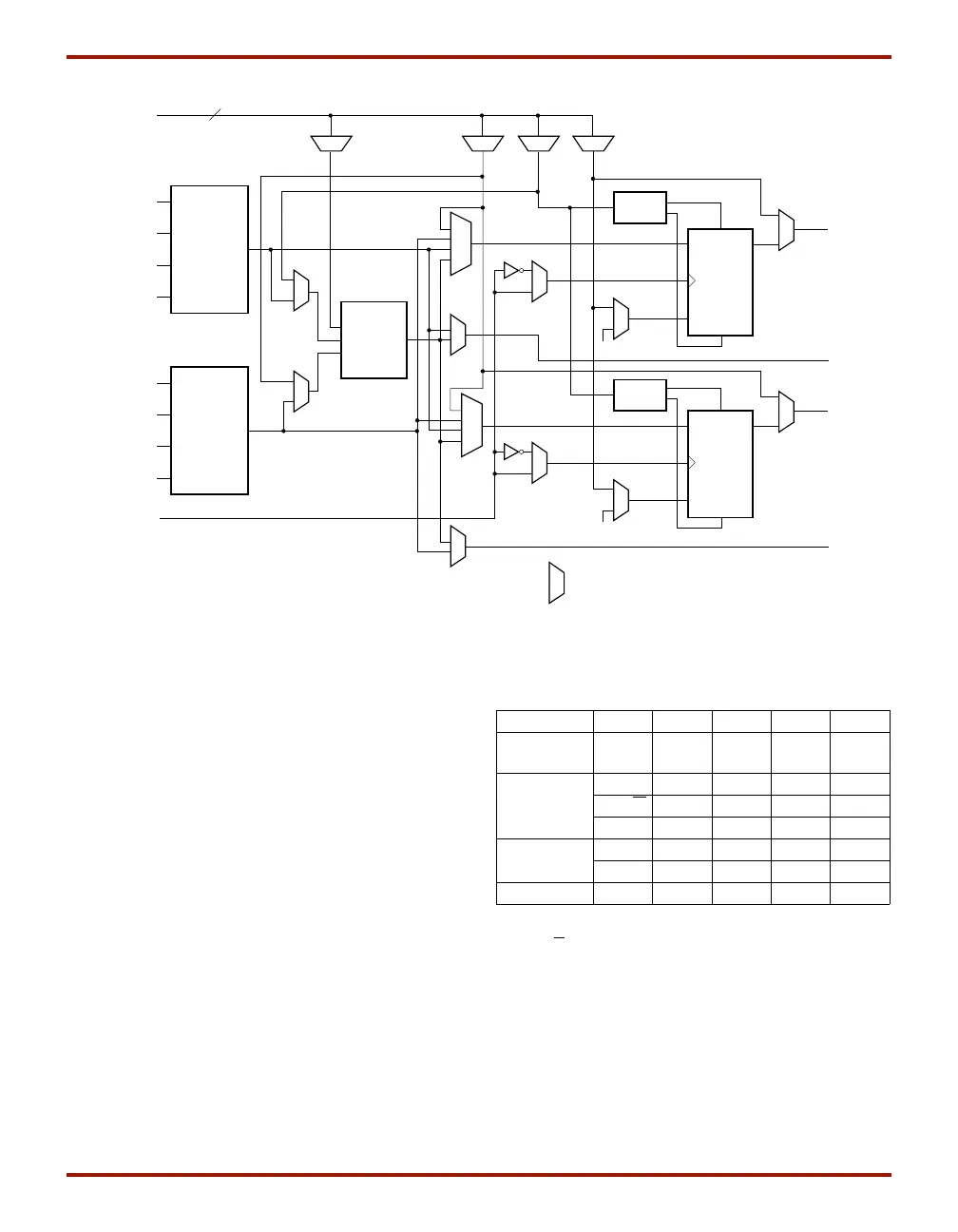
Flip-Flops
The CLB can pass the combinatorial output(s) to the inter-
connect network, but can also store the combinatorial
results or other incoming data in one or two flip-flops, and
connect their outputs to the interconnect network as well.
The two edge-triggered D-type flip-flops have common
clock (K) and clock enable (EC) inputs. Either or both clock
inputs can also be permanently enabled. Storage element
functionality is described in Table 4.
Latches (XC4000EX only)
The CLB storage elements can also be configured as
latches. The two latches have common clock (K) and clock
enable (EC) inputs. Storage element functionality is
described in Table 4.
Clock Input
Each flip-flop can be triggered on either the rising or falling
clock edge. The clock pin is shared by both storage ele-
ments. However, the clock is individually invertible for each
storage element. Any inverter placed on the clock input is
automatically absorbed into the CLB.
LOGIC
FUNCTION
OF
G1-G4
G
4
G
3
G
2
G
1
G'
LOGIC
FUNCTION
OF
F1-F4
F
4
F
3
F
2
F
1
F'
LOGIC
FUNCTION
OF
F', G',
AND
H1
H'
DIN
F'
G'
H'
DIN
F'
G'
H'
G'
H'
H'
F'
S/R
CONTROL
D
EC
RD
Bypass
Bypass
SD
YQ
XQ
Q
S/R
CONTROL
D
EC
RD
SD
Q
1
1
K
(CLOCK)
Multiplexer Controlled
by Configuration Program
Y
X
D
IN
/H
2
H
1
SR/H
0
EC
X6692
C
1
• • • C
4
4
Figure 1: Simplified Block Diagram of XC4000-Series CLB (RAM and Carry Logic functions not shown)
Table 4: CLB Storage Element Functionality
(active rising edge is shown)
Mode K EC SR D Q
Power-Up or
GSR
XXXXSR
Flip-Flop
XX1XSR
__/ 1* 0* D D
0X0*XQ
Latch
11*0*XQ
01*0*DD
Both X 0 0* X Q
Legend:
X
__/
SR
0*
1*
Don’t care
Rising edge
Set or Reset value. Reset is default.
Input is Low or unconnected (default value)
Input is High or unconnected (default value)
 Loading...