Do you have a question about the Yaesu FRG-7700 and is the answer not in the manual?
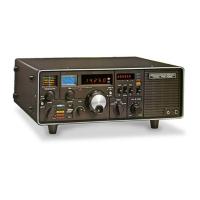
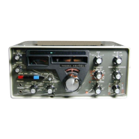
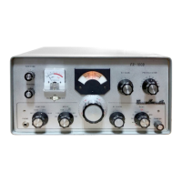
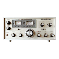
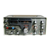
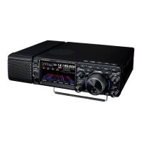
Overview of the FRG-7700 general coverage communications receiver, highlighting its features and capabilities.
Technical specifications of the FRG-7700, including frequency range, modes, sensitivity, selectivity, and power requirements.
Lists integrated circuits (ICs), transistors, diodes, and LEDs used in the FRG-7700.
Details optional accessories available for the FRG-7700, such as LF filters and antennas.
Identifies and explains the function of front and rear panel controls and switches on the FRG-7700.
Step-by-step instructions for setting up and installing the FRG-7700 receiver.
Guide to operating the FRG-7700, covering frequency selection, reception modes, and memory functions.
Overall block diagram illustrating the FRG-7700's functional units and signal flow.
Detailed block diagram of the Phase Locked Loop (PLL) unit.
Detailed explanation of the FRG-7700's circuit operation, including receiver signal flow and noise blanker.
Table listing crystal specifications, including function, holder, range, mode, load capacitance, and drive level.
Schematic diagram for the FRT-7700 unit, showing component interconnections.
Circuit diagram for the FF-5 LF filter, illustrating its internal components and connections.
Circuit diagram for the FRV-7700, detailing its electronic components and layout.
Schematic diagram for the FRA-7700 antenna, showing its circuit design.
Instructions for installing the DC power supply kit, including parts and procedures.
Describes a modification to correct a 1 kHz error in memory frequency recall.
Details a modification to improve performance on earlier FRG-7700 models.
Instructions for removing the front panel of the FRG-7700.
Steps for safely removing the rear panel of the FRG-7700.
Procedure for removing the outer casing of the FRG-7700 unit.
Component layout diagram for the main unit (PB-2169) of the FRG-7700.
Component placement diagram for the PLL unit (PB-2170).
Top and bottom views of the FRG-7700 main unit board layout.
Component layout for the VFO unit (PB-2172).
Component placement diagram for the FM unit (PB-2176).
Component layout for the Power Supply unit (PB-2171).
Component placement diagram for the Switch unit (PB-2173).
Component layout diagram for the Memory unit (PB-2175).
Schematic diagram for the FRG-7700 memory unit.
Waveform charts for various points within the memory unit.
Timing chart illustrating signal sequences in the memory unit.
Table showing PLL VCO selection settings for different bands.
Table detailing PLL dividing ratios for the Q2042.
Table for selecting Band Pass Filters (BPF) on the main unit.
Diagrams showing band switch contact positions for S1 and S2.
Techniques and precautions for soldering and desoldering on printed circuit boards.
Procedures for routine maintenance and alignment of the FRG-7700.
Troubleshooting guide with flowcharts for common FRG-7700 problems.
Forms and instructions for ordering replacement parts for the FRG-7700.
Comprehensive list of all repair parts for the FRG-7700, including part numbers and descriptions.
Step-by-step guide for installing the FRT-7700 antenna tuner.
Instructions for operating the FRT-7700 antenna tuner.
Procedure for installing the FF-5 LF filter onto the FRG-7700.
Details on connecting the FF-5 LF filter to the FRG-7700.
| Image Rejection | 70 dB |
|---|---|
| IF Rejection | 70 dB |
| Frequency Range | 150 kHz to 30 MHz |
| Modes | AM, SSB, CW |
| Selectivity | 6 kHz |
| IF Frequency | 455 kHz |