EasyManua.ls Logo

Yamaha Clavinova CVP-98 User Manual

Yamaha Clavinova CVP-98
178 pages
To Next Page IconTo Next Page
Page #1 background imageLoading...
Page #1 background image
Clavinova.
CVP-SS/CVP-9B
CL
I001587 I
SERVICE MANUAL
CVP-96
CVP-98
CONTENTS(§~)
SPECIFICATIONS
(nlf€~1±tl)
............................................• ,
..
2/3
PANEL
LAYO.UT
(l~*Jvv1'
J'r';J
1--)
....................................... 4
CIRCUIT BOARD LAYOUT
P-=
·:;
1--
v1'
7'r'J
l--):CVP-96 ..... 6
CIRCUIT BOARD LAYOUT
P-=
·:;
1--
v1'
7'
ry
l--):CVP-98 .... : 9
BLOCK DIAGRAM
("~:
D ::
-7
~:
1'
~
~:?
b.) :CVP-96 .......... / 12
BLOCK DIAGRAM ( 7 D
:;
-7
5i
1'
;
/J
7 b.).CVP-98 ··'.····,······ 14
DISASSEMBLY PROCEDURE (7tM-¥Jili):CVP-96 .... : .......... 16
DISASSEMBLY PROCEDURE (7t~-¥ili~):CVP-98 ............... 28
LSI
PIN DESCRIPTION (LSlll/M-=fiUi~~) ............................... 40
IC
BLOCK DIAGRAM
(IC
:f
o
·:;
-7
&I)
.................................... 45
CIRCUIT BOARDS
(:.t-
1--~~&&I)
........................................ 46
TEST PROGRAM
(7
A 1--7°01' 7 b.) .............................. 72/74
INSPECTIONS
(~~)
........................................................ 75/77
MESSAGE (
:;<
·:;
-tz-
~.i'-J;i) ............................................. 78/82
CONNECTING CABLES
(~~J;--:iJvf;,cfJR&I) ..................... 86
MIDI DATA FORMAT
(MIDIT'-9
7
~-7
·:;
1--)
.................. 87
MIDI IMPLEMENTATION CHART ........................................ 103
PARTS LIST
YAMAHA
CORP.
HAMAMATSU,
JAPAN
2.26K-7641
@)
Printed
in
Japan
'97.07
Question and Answer IconNeed help?

Do you have a question about the Yamaha Clavinova CVP-98 and is the answer not in the manual?
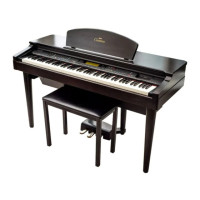
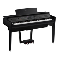
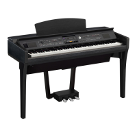
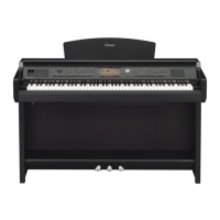
Yamaha Clavinova CVP-98 Specifications

General IconGeneral
Number of Keys88
Sound SourceAWM (Advanced Wave Memory)
EffectsReverb, Chorus, DSP
Sequencer16-track
DisplayLCD
ConnectivityMIDI, AUX IN, AUX OUT, Headphones, USB
Included AccessoriesBench, Music Rest, Owner's Manual, Power Cord
Polyphony64 notes

Summary

Specifications Overview

Block Diagram (CVP-96)

DM and CPU Block Diagram (CVP-96)

Functional block diagram illustrating the data flow and connections for the DM and CPU sections.

CVP-96 Disassembly Procedures

Top Board Assembly Removal

Step-by-step instructions for removing the top board assembly, including screw locations.

LSI Pin Description (LSI端子機能表)

HD6437043E00F (XS936A00) CPU Pin Description

Detailed pin assignments and functions for the CPU LSI.

LSI Pin Description (Continued)

IC Block Diagram (ICブロック図)

Schematic diagrams showing the internal structure of various ICs used in the unit.

Test Program

Test Program Preparation

Required instruments, jigs, unit settings, and initial steps for performing tests.

How to Enter and Proceed Through Test Program

Instructions on how to enter test mode, select programs, start tests, and interpret results.

Inspections

Audio Input/Output Checks

Procedures for testing AUX inputs and outputs using sine wave signals and measuring levels.

MIDI Data Format

Transmit and Receive Flow

Tables detailing MIDI messages transmitted and received for various functions, including control and system data.

MIDI Implementation Chart

Transmitted and Recognized MIDI Messages

A comprehensive chart showing MIDI messages transmitted and recognized by the unit.

Overall Circuit Diagram 1/5 (DM, MIC, PEDAL-VR, PEDAL)

DM Block Diagram

Schematic diagram illustrating the DM section, including CPU and related components.

Overall Circuit Diagram 2/5 (PNL, PNR, PNGL, PNGC, PNGR, MV, INV)

PNL and MV Circuit Diagrams

Schematics for the PNL and MV circuit boards, showing component layouts and connections.

PNR, PNGL, PNGC, PNGR Circuit Diagrams

Schematic diagrams for PNR, PNGL, PNGC, and PNGR circuit boards.

Overall Circuit Diagram 2/5 (Continued)

INV Circuit Diagram

Schematic diagram illustrating the INV circuit board and its connections.

Overall Circuit Diagram 3/5 (MA120, FU240, NET1)

MA120 Circuit Diagram

Schematic illustration of the MA120 assembly, showing its internal circuitry and connections.

FU240 and NET1 Circuit Diagrams

Schematics for the FU240 and NET1 circuit boards, detailing component layouts.

Overall Circuit Diagram 4/5 (EQ, JACK1, HP, PL)

Overall Circuit Diagram 4/5 (Continued)

Overall Circuit Diagram 5/5 (EQ, JACK1, HP, PL, AEXL88H, AEXL88L)

Overall Circuit Diagram 5/5 (Continued)

Related product manuals