EasyManua.ls Logo

Yamaha DSP-AX3900 User Manual

Yamaha DSP-AX3900
226 pages
To Next Page IconTo Next Page
Page #1 background imageLoading...
Page #1 background image
RX-V3900/
DSP-AX3900
101115
SERVICE MANUAL
IMPORTANT NOTICE
This manual has been provided for the use of authorized YAMAHA Retailers and their service personnel.
It has been assumed that basic service procedures inherent to the industry, and more speci cally YAMAHA Products, are already known
and understood by the users, and have therefore not been restated.
WARNING:
Failure to follow appropriate service and safety procedures when servicing this product may result in personal injury,
destruction of expensive components, and failure of the product to perform as speci ed. For these reasons, we advise
all YAMAHA product owners that any service required should be performed by an authorized YAMAHA Retailer or
the appointed service representative.
IMPORTANT:
The presentation or sale of this manual to any individual or rm does not constitute authorization, certi cation or
recognition of any applicable technical capabilities, or establish a principle-agent relationship of any form.
The data provided is believed to be accurate and applicable to the unit(s) indicated on the cover. The research, engineering, and service
departments of YAMAHA are continually striving to improve YAMAHA products. Modifications are, therefore, inevitable and
speci cations are subject to change without notice or obligation to retro t. Should any discrepancy appear to exist, please contact the
distributor's Service Division.
WARNING:
Static discharges can destroy expensive components. Discharge any static electricity your body may have
accumulated by grounding yourself to the ground buss in the unit (heavy gauge black wires connect to this buss).
IMPORTANT:
Turn the unit OFF during disassembly and part replacement. Recheck all work before you apply power to the unit.
CONTENTS
TO SERVICE PERSONNEL ........................................2–3
FRONT PANELS .........................................................3–4
REAR PANELS ...........................................................5–8
REMOTE CONTROL PANELS .......................................9
SPECIFICATIONS /
参考仕様
................................. 10–15
INTERNAL VIEW .......................................................... 16
DISASSEMBLY PROCEDURES /
分解手順
........... 17–25
UPDATING FIRMWARE /
ファームウェアの書き込み
.....................................26–29
SELF-DIAGNOSTIC FUNCTION /
ダイアグ(自己診断機能)
.......................................30–82
AMP ADJUSTMENT /
アンプ部調整
.............................83
DISPLAY DATA .......................................................84–85
IC DATA ................................................................. 86–103
BLOCK DIAGRAMS ............................................ 104–108
PIN CONNECTION DIAGRAMS ..........................109–111
PRINTED CIRCUIT BOARDS ............................. 112–143
SCHEMATIC DIAGRAMS ................................... 145–170
REPLACEMENT PARTS LIST ............................ 171–212
REMOTE CONTROL ........................................... 213–216
ADVANCED SETUP /
本機の設を変更す
...... 217–224
AV RECEIVER/AV AMPLIFIER
animate '08.10
P.O.Box 1, Hamamatsu, Japan
Copyright © 2008 All rights reserved.
This manual is copyrighted by YAMAHA and may not be copied or
redistributed either in print or electronically without permission.
RX-V3900/DSP-AX3900

Table of Contents

Question and Answer IconNeed help?

Do you have a question about the Yamaha DSP-AX3900 and is the answer not in the manual?

Yamaha DSP-AX3900 Specifications

General IconGeneral
Audio Channels7.1
Frequency Response10 Hz - 100 kHz +0, -3 dB
Input Sensitivity200mV/47kΩ (LINE)
Signal to Noise Ratio100 dB
Digital InputsOptical, Coaxial
Video InputsComponent, Composite, S-Video
Video OutputsComponent, Composite, S-Video
OutputsComponent, Composite, S-Video

Summary

Important Service Information and Warnings

Service Personnel Guidelines

Critical Components and Leakage Current Measurement

Guidelines for replacing critical components and verifying insulation after servicing. Includes leakage current test procedures.

Chemical Content Notice and Solder Handling

Important safety notice regarding chemical content and proper handling of solder and related materials.

Front Panel Overview

Rear Panel Overview

Remote Control Panel Layouts

Technical Specifications

Audio Section Specifications

Detailed specifications for the audio output power, sensitivity, distortion, and frequency response.

Video Section Specifications

Specifications for video signal types, conversion, and signal levels, including NTSC/PAL and composite signals.

FM and AM Tuner Specifications

General Unit Specifications

Power Supply, Dimensions, Weight, and Accessories

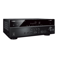
Details on power requirements, physical dimensions, weight, available finishes, and included accessories.

HDMI and Other Feature Information

DSP Selectable Sound Fields

Manual Setup Menu Overview

Speaker, Volume, and Sound Menu Settings

Configuration options for speakers, volume levels, dynamic range, tone controls, and lipsync.

Manual Setup Menu Options

Video, HDMI, Network, Multi Zone, and Option Settings

Settings for video conversion, HDMI, network, multi-zone audio, and general operational options.

Internal View of Components

Disassembly Procedures

Top Cover, Front Panel, and Sub Chassis Removal

Step-by-step instructions for removing major external and internal chassis components.

Printed Circuit Board (P.C.B.) Checking Procedures

P.C.B. Removal Procedures

D-VIDEO and A-VIDEO P.C.B. Removal

Detailed steps for safely removing the D-VIDEO and A-VIDEO printed circuit boards.

Rear Unit Removal Procedure

P.C.B. Checking Procedures (Continued)

Amplifier Unit Removal Procedure

P.C.B. Checking Procedures (Continued)

Firmware Update Procedures

Required Tools and Operation Steps

List of necessary tools and step-by-step instructions for updating the unit's firmware.

Firmware Update Completion and Error Handling

Firmware Update Error Displays

Explanation of common error messages encountered during firmware updates and their meanings.

Firmware Version and Checksum Confirmation

Self-Diagnostic Function Overview

Main Menu and Sub-Menu Listings

A comprehensive list of main menus and their corresponding sub-menus for self-diagnosis.

Starting Self-Diagnostic Functions

Entering Self-Diagnostic Mode with Protection Disabled

Procedure to enter self-diagnostic mode while disabling protection functions.

Entering Self-Diagnostic Mode

Standard procedure to access the unit's self-diagnostic mode.

Self-Diagnostic Function Display Information

Displaying Protection History Status

Information on how protection history is displayed based on different conditions.

Protection History Details and Causes

Protection History Due to Speaker Terminal Short

Explanation and display for protection triggered by speaker terminal shorts.

Protection History Due to Abnormal Voltage

Explanation and display for protection triggered by abnormal power supply voltages.

Protection History Details and Causes (Continued)

Protection History Due to Abnormal DC Output

Explanation and display for protection triggered by abnormal DC output.

Protection History Due to Excessive Heat Sink Temperature

Explanation and display for protection triggered by excessive heat sink temperatures.

Protection History Function Explanation

Information on how protection history is stored, cleared, and its implications.

Self-Diagnostic Menu Operation

Display and Operation Procedures for Menus

How information is displayed and how to navigate through main and sub-menus.

Self-Diagnostic Functionality and Settings

Functions Available and Initial Settings

Details on functions available during self-diagnostics and their initial default settings.

Input Changes During Menu Selection

Information on how input sources automatically change when navigating menus.

Self-Diagnostic Menu Details

A: Audio Settings Details

Detailed explanations for audio-related self-diagnostic functions.

A1. DSP THROUGH Function Details

Specific details and operation of the DSP THROUGH function.

Self-Diagnostic Menu Details (Continued)

A2. BYPASS Functions Details

Detailed explanations for Analog Bypass and DSP Bypass functions.

Self-Diagnostic Menu Details (Continued)

A3. HDMI AUDIO Settings

Configuration for HDMI audio signal selection and output.

A4. SPEAKERS SET Configuration

Settings for configuring speaker output levels and characteristics.

Speaker Settings Explanations

A5. MULTI CH INPUT Settings

A6. FL/OSD CHECK Procedure

A6. MIC CHECK Procedure

A7. MANUAL TEST Function

G: Graphic (Display System) Checks

G1. FL CHECK Procedure

Step-by-step guide to check the front panel FL display functionality.

Z: Zone Function Confirmation

Z1. ZONE TEST Procedures

Tests for confirming audio output to different zones based on selected input sources.

R: Radio Tuner Functions

R1. XM TEST Procedure

Procedure for testing XM radio reception and antenna.

R2. SIRIUS TEST Procedure

R3. HD RADIO TEST Procedure

U: Universal Terminal System

U1. DOCK Connector Test

Procedure to test the DOCK connector's functionality, including iPod detection.

U2. USB Check Procedures

USB File Playback Procedures

N: Network Function System

N1. NET CHECK Procedures

Procedures for checking network connection status, IP address, and MAC address.

MAC Address Setting Procedures

LINK CHECK Procedure

Network Connector Tests

External Loopback and PHY Tests

Procedures for testing network connector loopback and PHY connections.

Line Noise Measurement

Instructions for measuring line noise at 10Mbps and 100Mbps.

C: Communication Checks

C1. FUNCTION P.C.B. CHECK

Checking the FUNCTION PCB for data transmission and flow port.

C2. DSP P.C.B. CHECK

TI1 (DSP1) BUS Check

Checking the bus line connection for the TI1 (DSP1) IC.

TI2 (DSP2) BUS Check

Checking the bus line connection for the TI2 (DSP2) IC.

C3. D-VIDEO P.C.B. CHECK

ALL Check and Bus Line Checks

Performing comprehensive checks on SDRAM, NPGA, YGV, and I2C bus lines.

FPGA and EEPROM Checks

FPGA BUS and EEPROM Checks

Checking the connection of FPGA SPI line and EEPROM I2C line.

C4. HDMI Information

HDMI Model Name, Product ID, and Vendor Name

Displaying information about the HDMI module, including model, product ID, and vendor.

C5. EPROM CHECK

V: Video System

V1. A-VIDEO P.C.B. CHECK

Checking the A-VIDEO PCB for video signal conversion and output.

Video Signal Paths

DIGITAL BYPASS and REC ZONE Signal Paths

Diagrams illustrating signal paths for digital bypass and REC ZONE functions.

Video Signal Paths (Continued)

TEST PATTERN Display

Procedure for checking the FL display with various test patterns.

VIDEO INFO Display

Displaying information about the current input video signal.

D-VIDEO P.C.B. ROUTE CHECK

HDMI Loop-back Test Procedures

Detailed steps for performing HDMI loop-back tests (TEST1 and TEST2).

Video Signal Path Tests

TEST3 and TEST4 Procedures

Testing signal paths for different video resolutions and formats.

HDMI Signal Path Details

HDMI to HDMI_out1 Signal Path

Diagram illustrating the signal flow from HDMI input to HDMI output.

CVBS to DA and HDMI_out1 Signal Path

Diagram illustrating the signal flow from CVBS input to DA and HDMI output.

Video Signal Path Details (Continued)

CVBS to DA and HDMI_out1 with DDR Signal Path

Diagram illustrating the signal path from CVBS input to DA and HDMI output with DDR.

Y/C to DA and HDMI_out1 Signal Path

Diagram illustrating the signal path from Y/C input to DA and HDMI output.

Video Signal Path Details (Continued)

Component_480p to DA and HDMI_out1 Signal Path

Diagram illustrating the signal path from Component 480p to DA and HDMI_out1.

Component_720p to HDMI_out1 Signal Path

Diagram illustrating the signal path from Component 720p to HDMI_out1.

Video Signal Path Details (Continued)

YGV to DA and HDMI_out1 Signal Path

Diagram illustrating the signal path from YGV to DA and HDMI_out1.

P: Power Supply System

P1. SYSTEM MONITOR

Monitoring A/D conversion values for panel keys and protection functions.

Power Supply Monitoring Details

Temperature Detection Monitoring

Monitoring heat sink temperatures (TM1 and TM2) for proper operation.

Output Level and Limiter Control Monitoring

Monitoring amplifier output level (OUTLVL) and limiter control value (LMTCNT).

Amplifier Power Control (AMPPOW)

Controlling amplifier power relay states using the PURE DIRECT key.

Model and Destination Detection

MODEL and DESTINATION Detection Values

Displays detected model and destination information based on voltage readings.

Panel Key (K0/K1) Function Check

P2. PROTECTION HIST. Function

S: System Settings

S1. FIRM UPDATE Confirmation

Confirmation procedures for firmware updates across different microprocessors.

S2. TOOL UPDATE Confirmation

Confirmation procedures for tool updates like CEC MCU and HD RADIO MOD.

S3. FACTORY PRESET Settings

Preset Station Data Table

Table for recording FM and AM preset station data.

Preset Reserved and Preset Inhibit Options

Options to reserve or inhibit factory preset initialization for user memory protection.

S4. ROM VER/SUM Display

S5. SET INFO. Display

S6. SOFT SW Information

Amplifier Adjustment Procedures

Idling Current Confirmation for Amplifier Unit

Procedure to confirm and adjust amplifier idling current after repair.

Display Data and Pin Connections

IC Pin Connection Diagrams

Pinout diagrams for various integrated circuits used in the unit.

IC Data Information

IC534, 567: D70YE101BRFP266 (DSP P.C.B.) Details

Detailed information for the DSP IC, including its functions and pin assignments.

Block Diagrams

Audio Section Block Diagram

Overall block diagram illustrating the audio signal processing path.

Video Section Block Diagram

D-VIDEO Section Block Diagram

Power Section Block Diagram

Control Section Block Diagram

Pin Connection Diagrams

Integrated Circuit (IC) Pinouts

Pinout diagrams for various integrated circuits used in the unit.

Printed Circuit Board (P.C.B.) Layouts

DSP P.C.B. Layouts (Side A)

Layout diagram of the DSP printed circuit board, Side A.

DSP P.C.B. Layouts (Side B)

FUNCTION P.C.B. Layouts (Side A)

FUNCTION P.C.B. Layouts (Side B)

FUNCTION P.C.B. Layouts (Side A)

FUNCTION P.C.B. Layouts (Side B)

OPERATION P.C.B. Layouts

OPERATION P.C.B. Layouts (Side A)

Layout diagrams for various OPERATION PCBs, Side A.

OPERATION P.C.B. Layouts (Continued)

OPERATION P.C.B. Layouts (Side B)

Layout diagrams for various OPERATION PCBs, Side B.

OPERATION (3) P.C.B. Layouts

OPERATION (3) P.C.B. (Side A)

Layout diagram of the OPERATION (3) PCB, Side A.

OPERATION (3) P.C.B. Layouts (Continued)

OPERATION (3) P.C.B. (Side B)

Layout diagram of the OPERATION (3) PCB, Side B.

MAIN P.C.B. Layouts

MAIN (1) P.C.B. (Side A)

Layout diagram of the MAIN (1) PCB, Side A.

MAIN P.C.B. Layouts (Continued)

MAIN (1) P.C.B. (Side B)

Layout diagram of the MAIN (1) PCB, Side B.

MAIN P.C.B. Layouts (Continued)

MAIN (2), (3), (4) P.C.B. Layouts (Side A)

Layout diagrams for MAIN (2), (3), and (4) PCBs, Side A.

MAIN P.C.B. Layouts (Continued)

MAIN (2), (3), (4) P.C.B. Layouts (Side B)

Layout diagrams for MAIN (2), (3), and (4) PCBs, Side B.

POWER P.C.B. Layouts

POWER (1) P.C.B. Layouts (Side A & B)

Layout diagrams for the POWER (1) PCB, both sides.

POWER P.C.B. Layouts (Continued)

POWER (2), (5), (6) P.C.B. Layouts (Side A)

Layout diagrams for POWER (2), (5), and (6) PCBs, Side A.

POWER (5) P.C.B. Layouts (Side B)

Layout diagram for the POWER (5) PCB, Side B.

POWER P.C.B. Layouts (Continued)

POWER (3) P.C.B. Layouts (Side A & B)

Layout diagrams for the POWER (3) PCB, both sides.

POWER P.C.B. Layouts (Continued)

POWER (4) P.C.B. Layouts (Side A & B)

Layout diagrams for the POWER (4) PCB, both sides.

A-VIDEO P.C.B. Layouts

A-VIDEO P.C.B. (Side A)

Layout diagram of the A-VIDEO PCB, Side A.

A-VIDEO P.C.B. Layouts (Continued)

A-VIDEO P.C.B. (Side B)

Layout diagram of the A-VIDEO PCB, Side B.

D-VIDEO P.C.B. Layouts

D-VIDEO P.C.B. (Side A)

Layout diagram of the D-VIDEO PCB, Side A.

D-VIDEO P.C.B. Layouts (Continued)

D-VIDEO P.C.B. (Side B)

Layout diagram of the D-VIDEO PCB, Side B.

FL (1) P.C.B. Layouts

FL (1) P.C.B. (Side A)

Layout diagram of the FL (1) PCB, Side A.

FL (1) P.C.B. Layouts (Continued)

FL (1) P.C.B. (Side B)

Layout diagram of the FL (1) PCB, Side B.

FL (2) P.C.B. Layouts

FL (2) P.C.B. (Side A)

Layout diagram of the FL (2) PCB, Side A.

FL (2) P.C.B. Layouts (Continued)

FL (2) P.C.B. (Side B)

Layout diagram of the FL (2) PCB, Side B.

FL (3) & (4) P.C.B. Layouts

FL (3) & (4) P.C.B. (Side A)

Layout diagrams for FL (3) and (4) PCBs, Side A.

FL (3) & (4) P.C.B. (Side B)

Layout diagrams for FL (3) and (4) PCBs, Side B.

FL (5) & (6) P.C.B. Layouts

FL (5) & (6) P.C.B. (Side A)

Layout diagrams for FL (5) and (6) PCBs, Side A.

FL (5) & (6) P.C.B. (Side B)

Layout diagrams for FL (5) and (6) PCBs, Side B.

CONNECT (1) P.C.B. Layouts

CONNECT (1) P.C.B. (Side A & B)

Layout diagrams for the CONNECT (1) PCB, both sides.

CONNECT (2) P.C.B. Layouts

CONNECT (2) P.C.B. (Side A & B)

Layout diagrams for the CONNECT (2) PCB, both sides.

DCCNVT (1) P.C.B. Layouts

DCCNVT (1) P.C.B. (Side A & B)

Layout diagrams for the DCCNVT (1) PCB, both sides.

DCCNVT (2) P.C.B. Layouts

DCCNVT (2) P.C.B. (Side A & B)

Layout diagrams for the DCCNVT (2) PCB, both sides.

Schematic Diagrams

DSP Schematics (1/3)

Schematic diagram of the DSP section, part 1 of 3.

DSP Schematics (2/3)

DSP Schematics (3/3)

FUNCTION Schematics

FUNCTION 1/4 Schematic

Schematic diagram of the FUNCTION section, part 1 of 4.

FUNCTION Schematics (Continued)

FUNCTION 2/4 Schematic

Schematic diagram of the FUNCTION section, part 2 of 4.

FUNCTION Schematics (Continued)

FUNCTION 3/4 Schematic

Schematic diagram of the FUNCTION section, part 3 of 4.

FUNCTION Schematics (Continued)

FUNCTION 4/4 Schematic

Schematic diagram of the FUNCTION section, part 4 of 4.

OPERATION Schematics

OPERATION (1) through (7) Schematics

Schematic diagrams for all OPERATION PCBs, detailing component connections.

MAIN Schematics

MAIN (1) through (4) Schematics

Schematic diagrams for the MAIN PCBs, detailing component connections.

A-VIDEO Schematics

A-VIDEO 1/2 Schematic

Schematic diagram of the A-VIDEO section, part 1 of 2.

A-VIDEO Schematics (Continued)

A-VIDEO 2/2 Schematic

Schematic diagram of the A-VIDEO section, part 2 of 2.

D-VIDEO Schematics

D-VIDEO 1/10 Schematic

Schematic diagram of the D-VIDEO section, part 1 of 10.

D-VIDEO Schematics (Continued)

D-VIDEO 2/10 Schematic

Schematic diagram of the D-VIDEO section, part 2 of 10.

D-VIDEO Schematics (Continued)

D-VIDEO 3/10 Schematic

Schematic diagram of the D-VIDEO section, part 3 of 10.

D-VIDEO Schematics (Continued)

D-VIDEO 4/10 Schematic

Schematic diagram of the D-VIDEO section, part 4 of 10.

D-VIDEO Schematics (Continued)

D-VIDEO 5/10 Schematic

Schematic diagram of the D-VIDEO section, part 5 of 10.

D-VIDEO Schematics (Continued)

D-VIDEO 6/10 Schematic

Schematic diagram of the D-VIDEO section, part 6 of 10.

D-VIDEO Schematics (Continued)

D-VIDEO 7/10 Schematic

Schematic diagram of the D-VIDEO section, part 7 of 10.

D-VIDEO Schematics (Continued)

D-VIDEO 8/10 Schematic

Schematic diagram of the D-VIDEO section, part 8 of 10.

D-VIDEO Schematics (Continued)

D-VIDEO 9/10 Schematic

Schematic diagram of the D-VIDEO section, part 9 of 10.

D-VIDEO Schematics (Continued)

D-VIDEO 10/10 Schematic

Schematic diagram of the D-VIDEO section, part 10 of 10.

FL (1) P.C.B. Schematic

FL (2) P.C.B. Schematic

CONNECT (1) P.C.B. Schematic

DCCNVT (1) P.C.B. Schematic

REPLACEMENT PARTS LIST

Electrical Component Warnings and Abbreviations

Important safety warnings for electrical components and a list of abbreviations used in the parts list.

P.C.B. DSP Part List

P.C.B. DSP Part List (Continued)

P.C.B. FUNCTION Part List

P.C.B. FUNCTION Part List (Continued)

P.C.B. FUNCTION Part List (Continued)

P.C.B. D-VIDEO Part List

P.C.B. D-VIDEO Part List (Continued)

P.C.B. D-VIDEO Part List (Continued)

P.C.B. FUNCTION Part List

P.C.B. FUNCTION Part List (Continued)

P.C.B. FUNCTION Part List (Continued)

P.C.B. POWER Part List

P.C.B. POWER Part List (Continued)

P.C.B. OPERATION and MAIN Part List

P.C.B. FUNCTION Part List

P.C.B. MAIN Part List

P.C.B. MAIN Part List (Continued)

P.C.B. POWER Part List

P.C.B. POWER Part List (Continued)

P.C.B. POWER Part List (Continued)

P.C.B. A-VIDEO Part List

P.C.B. A-VIDEO Part List (Continued)

P.C.B. A-VIDEO Part List (Continued)

P.C.B. A-VIDEO Part List (Continued)

P.C.B. D-VIDEO Part List

P.C.B. D-VIDEO Part List (Continued)

P.C.B. D-VIDEO Part List (Continued)

P.C.B. D-VIDEO Part List (Continued)

P.C.B. D-VIDEO Part List (Continued)

P.C.B. D-VIDEO Part List (Continued)

P.C.B. D-VIDEO Part List (Continued)

P.C.B. D-VIDEO Part List (Continued)

P.C.B. FUNCTION Part List

P.C.B. CONNECT and DCCNVT Part List

P.C.B. DCCNVT Part List

Overall Assembly Diagram

Included Accessories

Front Panel and Sub Chassis Unit Assembly

Amplifier Unit Assembly

Remote Control Information

Remote Control Models and Details

Details and diagrams for RAV386, RAV388, and RAV387 remote controls.

Remote Control Key Layout and Codes

Key Layout, Codes, and Basic Settings

Information on remote control key layout, codes, ID, zone, macro, and input source settings.

Advanced Setup Menu Navigation

Using the Advanced Setup Menu

Instructions on how to access and navigate the advanced setup menu.

Advanced Setup Menu Options

System Settings Recovery, Backup, and Initialization

Procedures for saving, restoring, and initializing system settings.

Sirius Parental Lock and MAC Address Filter

Settings for parental controls on Sirius and MAC address filtering for network access.

Advanced Setup Menu Options (Continued)

TV Format, HDMI Monitor Check, and Language Settings

Settings for TV format, HDMI monitor output, and display language.

Firmware Update Procedures

Instructions for updating the unit's firmware via USB or Network.

Resetting the System to Factory Defaults

Changing Advanced Setup Settings

Remote Sensor, RS-232C, and Remote Control ID Settings

Configuration options for remote sensor, RS-232C communication, and remote control ID.

Advanced Setup Menu Options (Continued)

Bi-Amp Setup, Settings Save/Recall, and Parameter Initialization

Configuration for bi-amp, saving/recalling settings, and resetting parameters.

MAC Address Filter, TV Format, and HDMI Monitor Check

Settings for MAC filtering, TV format, and HDMI monitor output check.

Advanced Setup Menu Options (Continued)

Display Language and Firmware Update Settings

Settings for display language selection and firmware update procedures.

Resetting All Settings to Factory Defaults

Related product manuals