ABCDEFGH I J
1
2
3
4
5
6
7
RX-V530/RX-V530RDS/HTR-5550/HTR-5550RDS/DSP-AX530
RX-V430/RX-V430RDS/HTR-5540/HTR-5540RDS/DSP-AX430
57
PTY SEEK
FUNCTION (1)
VP
VRB
MG
+5M
VRA
PSW
ADKEY2
ADKEY0
CEF0
REM1
ADKEY1
/BLK
SCKO
RXDF
CE
TXDO
CLKO
VCC
RESET
RXDO
CTSO
VSS
CNVSS
INPUT
OPERATION (1) P. C. B.
(Lead Type Device)
OPERATION (2) P. C. B.
(Lead Type Device)
OPERATION (3) P. C. B.
(Lead Type Device)
OPERATION (1) P. C. B.
(Surface Mount Device)
12 5 1920 29 696865
STEREOPRESET
TUNING
A/B/C/D/E
STANDBY
/ON
BASS
TREBLE
6CH INPUT
VOLUME
INPUT MODE
EON
RDS MODE/
FREQ
MODE START
FM/AM TUNING
MODE
MEMORY
PROGRAM
PRESET/TUNING
64
33
48
1
16
17
32
49
14
85
58
41
FUNCTION (1)
Flash µ-COM Write Connector
+12
-12
TIL
E
TIR
E
TOL
E
TOR
CNVSS
VSS
CTSO
RXDO
CE
Power Transformer
RESET
VCC
CLKO
TXDO
PSW
+5M
PSW
+5M
NC
F1
F2
NC
F1
F2
J703
R735
R734
C705
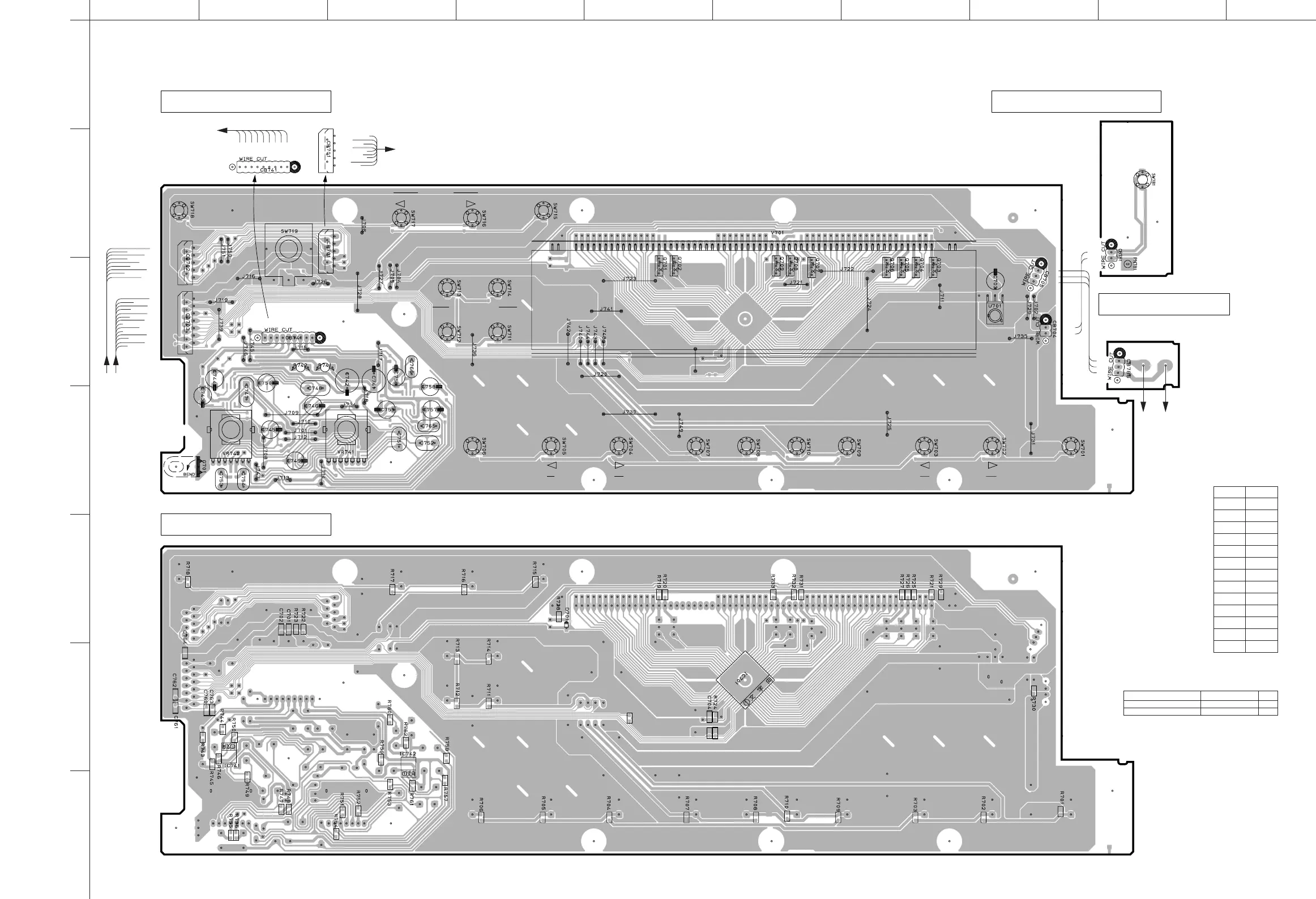
■ PRINTED CIRCUIT BOARD (Foil side)
• Semiconductor Location
Ref. No. Location
D701 D5
IC701 F6
IC741 B6
IC742 C6
Q701 E3
Q702 E3
Q703 G3
Q704 G3
Q705 G3
Q706 G3
Q707 F3
Q708 F3
Q709 F3
Circuit No. J, U, C, R, T, K, A, L B,G
R711~714 X O
SW711~714 X O
X: NOT USED
O: USED / APPLICABLE
 Loading...