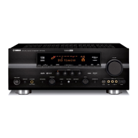
Do you have a question about the Yamaha DSP-AX861 and is the answer not in the manual?
Identifies components with special characteristics requiring exact replacement parts.
Verifies proper insulation of exposed surfaces from supply circuits after service.
Detailed specifications for the audio output power and performance characteristics.
Specifications related to video signal processing and compatibility.
Technical specifications for the FM tuner functionality.
Technical specifications for the AM tuner functionality.
Diagram showing the location of internal components when viewed from the top.
Step-by-step instructions for removing the top cover of the unit.
Instructions for safely removing the front panel assembly.
Procedure for disassembling and removing the sub-chassis unit.
Steps for removing the DSP and HDMI printed circuit boards.
Procedure for removing the FUNCTION (1) printed circuit board.
Instructions for removing the VIDEO printed circuit board.
Steps for removing the AM/FM tuner module.
Procedure for disassembling and removing the amplifier unit.
List of necessary software and hardware tools for firmware updates.
Step-by-step guide for performing firmware updates.
Verifying successful firmware update by checking version and checksum.
Procedure to reset the unit to default settings after firmware update.
Specific instructions for updating the firmware on the DSP module.
Instructions on how to initiate the diagnostic mode.
Procedure for exiting the diagnostic mode and returning to normal operation.
Guide on navigating and selecting options within the diagnostic menus.
Diagnostic option to test signal bypass functionality.
Diagnostic settings for speaker configuration and output levels.
Diagnostic test for the microphone input signal processing.
Diagnostic tool for checking the FL display and On-Screen Display.
Displays A/D conversion values for microprocessor inputs.
Diagnostic function to check the video circuit and signal paths.
Diagnostic test for the DOCK connector functionality.
Diagnostic option to select HDMI input signals for output.
Diagnoses the bus connection between DSP and external ROM/RAM.
Displays and allows adjustment of protection circuit settings.
Shows a record of past protection events and their status.
Allows software switching of function settings on PCBs.
Diagnostic option for initiating firmware updates.
Diagrams showing the pin assignments for various ICs.
Details for the digital audio interface transceiver IC.
Details for the floating-point digital signal processor IC.
Package diagrams and pinouts for various integrated circuits.
High-level diagram of the digital audio signal path.
High-level diagram of the analog audio signal path.
Diagram illustrating video and HDMI signal flow.
Diagram showing control signals and power distribution.
Layout diagram for the DSP printed circuit board, side B.
Layout diagram for the FUNCTION (1) printed circuit board, side A.
Layout diagram for the FUNCTION (2) printed circuit board, side A.
Layout diagram for the FUNCTION (4) printed circuit board, side A.
Layout diagram for the OPERATION (1) printed circuit board, side A.
Layout diagram for the OPERATION (1) printed circuit board, side B.
Layout diagram for the OPERATION (2) printed circuit board, side A.
Layout diagram for the MAIN (1) printed circuit board, side A.
Layout diagram for the MAIN (2) printed circuit board, side A.
Layout diagram for the VIDEO printed circuit board, side A.
Layout diagram for the HDMI printed circuit board, side A.
List of electrical components with part numbers for replacement.
Diagrams showing the layout of buttons on different remote control models.
Detailed guide for configuring advanced system settings.
Diagram illustrating how to connect devices for scene control.
Explanation of how the scene control function operates.
| Audio Channels | 7.1 |
|---|---|
| Amplifier Type | Discrete |
| HDMI Inputs | 4 |
| HDMI Outputs | 1 |
| Dolby Atmos | No |
| DTS:X | No |
| Signal-To-Noise Ratio | 100 dB |
| Total Harmonic Distortion | 0.06% |
| Total Harmonic Distortion (alternative) | 0.06 % |
| Input Impedance | 47 kΩ |
| Input Sensitivity | 200 mV |
| Audio D/A Converter | 192 kHz/24-bit |
| Surround Sound Effects | Yes |
| Sound Effects | Yes |
| DSP Presets | 17 |
| Tuner Bands | AM/FM |
| HDMI | Yes |
| Input Sensitivity/Impedance | 200 mV / 47 kΩ |
| Signal-to-Noise Ratio (CD) | 100 dB |
| Frequency Response | 10 Hz - 100 kHz |
| Response Bandwidth | 10 Hz - 100 kHz |
| HDMI Version | 1.3 |
| Built-in Decoders | Dolby Digital, DTS, Dolby Pro Logic IIx |
| Dimensions (W x H x D) | 435 mm x 171 mm x 437 mm |


