EasyManua.ls Logo

Yamaha DSP-AX750 User Manual

Yamaha DSP-AX750
128 pages
To Next Page IconTo Next Page
Page #1 background imageLoading...
Page #1 background image
This manual has been provided for the use of authorized YAMAHA Retailers and their service personnel.
It has been assumed that basic service procedures inherent to the industry, and more specifically YAMAHA Products, are already
known and understood by the users, and have therefore not been restated.
WARNING: Failure to follow appropriate service and safety procedures when servicing this product may result in personal
injury, destruction of expensive components, and failure of the product to perform as specified. For these reasons,
we advise all YAMAHA product owners that any service required should be performed by an authorized YAMAHA
Retailer or the appointed service representative.
IMPORTANT: The presentation or sale of this manual to any individual or firm does not constitute authorization, certification or
recognition of any applicable technical capabilities, or establish a principle-agent relationship of any form.
The data provided is believed to be accurate and applicable to the unit(s) indicated on the cover. The research, engineering, and service
departments of YAMAHA are continually striving to improve YAMAHA products. Modifications are, therefore, inevitable and
specifications are subject to change without notice or obligation to retrofit. Should any discrepancy appear to exist, please contact the
distributor's Service Division.
WARNING: Static discharges can destroy expensive components. Discharge any static electricity your body may have
accumulated by grounding yourself to the ground buss in the unit (heavy gauge black wires connect to this buss).
IMPORTANT: Turn the unit OFF during disassembly and part replacement. Recheck all work before you apply power to the unit.
IMPORTANT NOTICE
100885
SERVICE MANUAL
RX-V750/DSP-AX750/DSP-AX750SE
RX-V650/HTR-5760
AV RECEIVER/AV AMPLIFIER
AMP CHECK / アンプチェック . . . . . . . . . . . . . . . . . . . . 47
DISPLAY DATA . . . . . . . . . . . . . . . . . . . . . . . . . . 48–49
IC DATA . . . . . . . . . . . . . . . . . . . . . . . . . . . . . . . . 50–60
BLOCK DIAGRAM . . . . . . . . . . . . . . . . . . . . . . . . 61–62
PRINTED CIRCUIT BOARD . . . . . . . . . . . . . . . . 63–77
PIN CONNECTION DIAGRAM . . . . . . . . . . . . . . . . . 78
SCHEMATIC DIAGRAM . . . . . . . . . . . . . . . . . . . 79–88
PARTS LIST . . . . . . . . . . . . . . . . . . . . . . . . . . . . 89–125
REMOTE CONTROL RAV270, RAV271 . . . . 126–127
REMOTE CONTROL RAV248, RAV249 . . . . . . . . 128
CONTENTS
TO SERVICE PERSONNEL . . . . . . . . . . . . . . . . . . . . 2
IMPEDANCE SELECTOR . . . . . . . . . . . . . . . . . . . . . . 3
FRONT PANELS . . . . . . . . . . . . . . . . . . . . . . . . . . . 4–5
REMOTE CONTROL PANELS . . . . . . . . . . . . . . . . . . 6
REAR PANELS . . . . . . . . . . . . . . . . . . . . . . . . . . . 7–13
SPECIFICATIONS /
参考仕様 . . . . . . . . . . . . . . . . . 14–18
INTERNAL VIEW . . . . . . . . . . . . . . . . . . . . . . . . . . . . 19
DISASSEMBLY PROCEDURES /
分解手順 . . . . . 20–24
SELF DIAGNOSIS FUNCTION (DIAG) /
自己診断機能(ダイアグ) . . . . . . . . . . . . . . . . . . . . 25–46
RX-V750/DSP-AX750/DSP-AX750SE
RX-V650/HTR-5760
Question and Answer IconNeed help?

Do you have a question about the Yamaha DSP-AX750 and is the answer not in the manual?

Yamaha DSP-AX750 Specifications

General IconGeneral
TypeAV Receiver
Amplifier TypeDiscrete
Channels6.1
Total Harmonic Distortion (THD)0.06%
Input Sensitivity200 mV
Signal-to-Noise Ratio100 dB
Input Sensitivity/Impedance200 mV / 47 kOhms
Power Output100 W per channel (8 ohms)
Surround Sound FormatsDolby Digital, DTS
Signal to noise ratio100 dB
Digital Audio Inputs2 x Coaxial, 2 x Optical
Video ConnectionsComposite, S-Video, Component
Dimensions435 x 151 x 400 mm
Frequency Response10 Hz - 100 kHz

Summary

To Service Personnel

Critical Components Information

Notes on special components requiring exact replacement with specified parts.

Leakage Current Measurement

Procedure to verify insulation and measure leakage current for 120V models.

WARNING: CHEMICAL CONTENT NOTICE!

Warning about lead content in solder and other chemicals.

Impedance Selector

Caution

Precautions regarding lead-free solder and soldering iron usage.

WARNING: Do Not Change Impedance Selector Setting While Powered On

Warning against changing the impedance selector while the unit is powered on.

Front Panels

RX-V750 (U, C, R, T, K, A, G, L models)

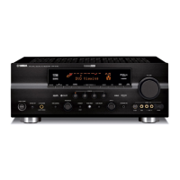
Front panel layout for RX-V750 models.

DSP-AX750 (J model)

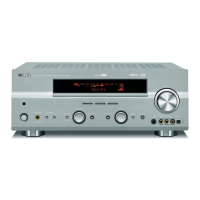
Front panel layout for DSP-AX750 (J model).

DSP-AX750SE (B model)

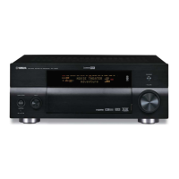
Front panel layout for DSP-AX750SE (B model).

Remote Control Panels

RAV270

Layout of RAV270 remote control.

RAV271

Layout of RAV271 remote control.

RAV248

Layout of RAV248 remote control.

RAV249

Layout of RAV249 remote control.

Rear Panels

RX-V750 (U, C models)

Rear panel layout for RX-V750 (U, C models).

RX-V750 (R model)

Rear panel layout for RX-V750 (R model).

RX-V750 (T model)

Rear panel layout for RX-V750 (T model).

Specifications / 参考仕様

AUDIO SECTION / オーディオ部

Audio output power and impedance specifications.

Maximum Power (EIAJ) / 実用最大出力

EIAJ maximum output power for different models and channels.

DIN Standard Output Power Per Channel (B, G, L, E models)

DIN standard output power for specific models.

Specifications / 参考仕様

IEC Power (B, G, L, E models)

IEC power ratings for specific models.

Dynamic Headroom (U, C models)

Dynamic headroom values for U, C models.

General / 総合

Power Supply / 電源電圧

Power supply voltage details for different models.

Power Consumption / 消費電力

Power consumption ratings for different models.

Set Menu Table / セットメニュー

AUTO SETUP

Settings for automatic setup of speaker configuration.

MANUAL SETUP

Manual setup options for sound and input settings.

OPTION MENU

Options for display settings and parameter initialization.

The Variable Range of the Parameter (MIN/MAX/STEP) / パラメーターの可変範囲

Internal View

SUB TRANS P.C.B.

Identification of Sub Trans PCB.

MAIN (2) P.C.B.

Identification of Main (2) PCB.

FM/AM TUNER (Except DSP-AX750SE)

Identification of FM/AM Tuner.

Disassembly Procedures / 分解手順

Removal of Top Cover

Steps to remove the top cover.

Removal of Front Panel

Steps to remove the front panel.

Disassembly Procedures / 分解手順

Removal of Sub Chassis

Steps to remove the sub chassis.

Disassembly Procedures / 分解手順

Removal of P.C.B. Unit

Steps to remove the PCB unit.

Disassembly Procedures / 分解手順

Operation check of MAIN (1) P.C.B.

Procedure for checking the operation of the MAIN (1) PCB.

Self Diagnosis Function (DIAG) / 自己診断機能(ダイアグ)

No. DIAG menu Sub-menu

List of DIAG menu items and their sub-menus.

Self Diagnosis Function (DIAG) / 自己診断機能(ダイアグ)

Starting DIAG

Procedure to activate the DIAG function.

Starting DIAG in the protection cancel mode

How to enter DIAG mode with protection function disabled.

CAUTION!

Cautionary note regarding using the product with protection disabled.

Self Diagnosis Function (DIAG) / 自己診断機能(ダイアグ)

Display provided when DIAG started

Display indications when DIAG starts on monitor and FL display.

When there is no protection history

Display message when no protection history is present.

Self Diagnosis Function (DIAG) / 自己診断機能(ダイアグ)

History of protection function

How protection function history is stored and cleared.

Display during menu operation

Display contents during DIAG operation.

Self Diagnosis Function (DIAG) / 自己診断機能(ダイアグ)

Operation procedure of DIAG MENU and SUB-MENU

How to navigate DIAG menus and sub-menus.

Functions in DIAG mode

Functions active during DIAG mode operation.

Details of DIAG menu

1. DSP THR

Explanation of DSP Threshold menu, margin/full bit output.

Details of DIAG menu

2. BYPASS

Explanation of Bypass menu, analog or DSP bypass output.

Details of DIAG menu

3. RAM THROUGH

Explanation of RAM Through menu, margin or full-bit output.

Details of DIAG menu

4. PRO LOGIC/NEO6

Explanation of Pro Logic/Neo6 settings.

Details of DIAG menu

5. SPEAKERS SET

Speaker setting options and their effects.

Details of DIAG menu

6. EXTERNAL INPUT

External input settings for multi-channel and impedance.

7. MIC CHECK

Microphone input signal check and display.

Details of DIAG menu

8. VFD CHECK

Procedure to check the FL display segment functionality.

Details of DIAG menu

9. MANUAL TEST

Manual test modes for outputting test noise to speakers.

Details of DIAG menu

10. FACTORY PRESET

Options for initializing backup RAM or preset memory.

PRESET STATIONS / プリセット局

Table of factory preset FM/AM station data.

Details of DIAG menu

11. AD DATA

Displays key scan, A/D values for protection ports, etc.

DC/PS (protection detection)

Details on DC and PS protection detection values.

THM/Fan

Temperature and fan status detection values.

Details of DIAG menu

IMP SW/POWER LIMIT (Impedance/power limiter detection)

Impedance and power limiter detection information.

K0/K1

A/D values for panel key input ports and their interpretation.

Details of DIAG menu

12. V CONV STATUS

Displays data received from the video conversion IC.

13. IF STATUS

Displays status information sequentially in hexadecimal notation.

Details of DIAG menu

<2nd byte> / <第 2 バイト>

Fs information of reproduction signal.

<3nd byte> / <第 3 バイト>

Audio code mode information of reproduction signal.

<4rd byte> / <第 4 バイト>

Format information of reproduction signal.

<5th byte> / <第5バイト>

Signal processing status information.

Details of DIAG menu

14. DSP RAM CHECK

Checks bus connection for YSS930 and external RAM.

15. PROTECTION SETTING

Protection setting (not applied to these models).

Details of DIAG menu

16. SOFT SWITCH

Switches function settings on PCB via software.

Details of DIAG menu

17. MICROPROCESSOR INFORMATION

Displays microprocessor information like version and checksum.

Amp Check / アンプチェック

CONFIRMATION OF IDLING CURRENT

Steps to measure and confirm idling current.

Display Data

PIN CONNECTION

Pin connection details for display components.

GRID ASSIGNMENT

Assignment of functions to grid segments.

Display Data

ANODE CONNECTION

Anode connection details for display components.

IC Data

IC2 : LC89057W-VF4D-E (DSP P.C.B.)

Data for the Digital Audio Interface Transceiver IC.

IC Data

IC2 : LC89057W-VF4D-E (DSP P.C.B.)

Pin functions for the Digital Audio Interface Transceiver IC.

IC Data

IC5 : YSS948-V (DSP P.C.B.)

Data for the ADAM IC.

IC Data

IC5 : YSS948-V (DSP P.C.B.)

Pin classification and function for the ADAM IC.

IC Data

IC5 : YSS948-V (DSP P.C.B.)

Pin functions for External Memory Interface, Status Port, and General Purpose I/O Port.

IC Data

IC5 : YSS948-V (DSP P.C.B.)

Continued pin functions for Test, Status Port, and General Purpose I/O.

IC Data

IC7 : YSS930-SZ (DSP P.C.B.)

Data for the DSP IC.

IC Data

IC7 : YSS930-SZ (DSP P.C.B.)

Pin functions for the DSP IC.

IC Data

IC502 : M30622MHP-161FP (FUNCTION P.C.B.)

Data for the 16-bit microcomputer IC.

IC Data

Key Input (A-D) Pull-Up Resistance 10 k-ohms

Pull-up resistance values for key inputs.

IC Data

IC606 : LC74781-9798 (FUNCTION P.C.B.)

Data for the On-screen Display Controller IC.

Block Diagram / ブロックダイアグラム

DSP

Block diagram of the DSP section.

OPERATION

Block diagram of the Operation section.

MAIN

Block diagram of the Main section.

FUNCTION

Block diagram of the Function section.

CONVERSION

Block diagram of the Conversion section.

Printed Circuit Board (Foil side)

DSP P.C.B. (Surface Mount Device)

Foil side view of DSP PCB (SMD components).

DSP P.C.B. (Lead Type Device)

Foil side view of DSP PCB (Lead components).

Printed Circuit Board (Foil side)

FUNCTION (1) P.C.B. (Lead Type Device)

Foil side view of Function (1) PCB (Lead components).

FUNCTION (1) P.C.B. (Surface Mount Device)

Foil side view of Function (1) PCB (SMD components).

Printed Circuit Board (Foil side)

FUNCTION (2) P.C.B. (Lead Type Device)

Foil side view of Function (2) PCB (Lead components).

FUNCTION (2) P.C.B. (Surface Mount Device)

Foil side view of Function (2) PCB (SMD components).

Printed Circuit Board (Foil side)

FUNCTION (2) P.C.B. (Lead Type Device)

Foil side view of Function (2) PCB (Lead components).

FUNCTION (7) P.C.B. (Lead Type Device)

Foil side view of Function (7) PCB (Lead components).

FUNCTION (3) P.C.B. (Lead Type Device)

Foil side view of Function (3) PCB (Lead components).

FUNCTION (4) P.C.B. (Lead Type Device)

Foil side view of Function (4) PCB (Lead components).

Printed Circuit Board (Foil side)

FUNCTION (2) P.C.B. (Lead Type Device)

Foil side view of Function (2) PCB (Lead components).

FUNCTION (1) P.C.B. (Lead Type Device)

Foil side view of Function (1) PCB (Lead components).

FUNCTION (6) P.C.B. (Lead Type Device)

Foil side view of Function (6) PCB (Lead components).

FUNCTION (7) P.C.B. (Lead Type Device)

Foil side view of Function (7) PCB (Lead components).

FUNCTION (7) P.C.B. (Surface Mount Device)

Foil side view of Function (7) PCB (SMD components).

FUNCTION (8) P.C.B. (Lead Type Device)

Foil side view of Function (8) PCB (Lead components).

Printed Circuit Board (Foil side)

OPERATION (1) P.C.B. (Lead Type Device)

Foil side view of Operation (1) PCB (Lead components).

OPERATION (1) P.C.B. (Surface Mount Device)

Foil side view of Operation (1) PCB (SMD components).

Printed Circuit Board (Foil side)

OPERATION (2) P.C.B. (Lead Type Device)

Foil side view of Operation (2) PCB (Lead components).

OPERATION (3) P.C.B. (Lead Type Device)

Foil side view of Operation (3) PCB (Lead components).

OPERATION (3) P.C.B. (Surface Mount Device)

Foil side view of Operation (3) PCB (SMD components).

OPERATION (4) P.C.B. (Lead Type Device)

Foil side view of Operation (4) PCB (Lead components).

OPERATION (4) P.C.B. (Surface Mount Device)

Foil side view of Operation (4) PCB (SMD components).

OPERATION (5) P.C.B. (Lead Type Device)

Foil side view of Operation (5) PCB (Lead components).

OPERATION (5) P.C.B. (Surface Mount Device)

Foil side view of Operation (5) PCB (SMD components).

Printed Circuit Board (Foil side)

OPERATION (1) P.C.B. (Lead Type Device)

Foil side view of Operation (1) PCB (Lead components).

OPERATION (1) P.C.B. (Surface Mount Device)

Foil side view of Operation (1) PCB (SMD components).

Printed Circuit Board (Foil side)

OPERATION (2) P.C.B. (Lead Type Device)

Foil side view of Operation (2) PCB (Lead components).

OPERATION (3) P.C.B. (Lead Type Device)

Foil side view of Operation (3) PCB (Lead components).

OPERATION (3) P.C.B. (Surface Mount Device)

Foil side view of Operation (3) PCB (SMD components).

OPERATION (4) P.C.B. (Lead Type Device)

Foil side view of Operation (4) PCB (Lead components).

OPERATION (4) P.C.B. (Surface Mount Device)

Foil side view of Operation (4) PCB (SMD components).

OPERATION (5) P.C.B. (Lead Type Device)

Foil side view of Operation (5) PCB (Lead components).

OPERATION (5) P.C.B. (Surface Mount Device)

Foil side view of Operation (5) PCB (SMD components).

OPERATION (6) P.C.B. (Lead Type Device)

Foil side view of Operation (6) PCB (Lead components).

OPERATION (6) P.C.B. (Surface Mount Device)

Foil side view of Operation (6) PCB (SMD components).

Printed Circuit Board (Foil side)

MAIN (1) P.C.B. (Lead Type Device)

Foil side view of Main (1) PCB (Lead components).

MAIN (5) P.C.B. (Lead Type Device)

Foil side view of Main (5) PCB (Lead components).

Printed Circuit Board (Foil side)

MAIN (2) P.C.B. (Lead Type Device)

Foil side view of Main (2) PCB (Lead components).

MAIN (3) P.C.B. (Lead Type Device)

Foil side view of Main (3) PCB (Lead components).

MAIN (6) P.C.B. (Lead Type Device)

Foil side view of Main (6) PCB (Lead components).

Printed Circuit Board (Foil side)

POWER (1) P.C.B. (Lead Type Device)

Foil side view of Power (1) PCB (Lead components).

POWER (2) P.C.B. (Lead Type Device)

Foil side view of Power (2) PCB (Lead components).

Printed Circuit Board (Foil side)

SUB TRANS P.C.B. (Lead Type Device)

Foil side view of Sub Trans PCB (Lead components).

Printed Circuit Board (Foil side)

CONVERSION (1) P.C.B. (Lead Type Device)

Foil side view of Conversion (1) PCB (Lead components).

CONVERSION (1) P.C.B. (Surface Mount Device)

Foil side view of Conversion (1) PCB (SMD components).

CONVERSION (2) P.C.B. (Lead Type Device)

Foil side view of Conversion (2) PCB (Lead components).

CONVERSION (2) P.C.B. (Surface Mount Device)

Foil side view of Conversion (2) PCB (SMD components).

Pin Connection Diagram / 半導体外形図

ICs

Pin connection diagrams for various ICs.

Transistors

Physical outlines of transistors.

FETs

Physical outlines of FETs.

Diodes

Physical outlines of diodes.

Schematic Diagram (DSP)

Schematic Diagram (FUNCTION 1/2)

Schematic Diagram (FUNCTION 2/2)

Schematic Diagram (OPERATION)

CPU

Schematic of the CPU and related circuits.

Schematic Diagram (OPERATION)

DISPLAY DRIVER

Schematic of the display driver circuit.

Schematic Diagram (MAIN)

Schematic Diagram (POWER & SUB TRANS)

Schematic Diagram (CONVERSION)

Parts List

ELECTRICAL PARTS

List of electrical components with part numbers and descriptions.

WARNING

Warning about replacing critical components with exact specifications.

Parts List

P.C.B. DSP

Parts list for the DSP PCB.

Parts List

P.C.B. DSP & FUNCTION

Parts list for DSP and Function PCBs.

Parts List

P.C.B. FUNCTION

Parts list for Function PCBs.

Parts List

P.C.B. MAIN & POWER

Parts list for Main and Power PCBs.

Parts List

P.C.B. OPERATION

Parts list for Operation PCBs.

Parts List

P.C.B. MAIN

Parts list for the Main PCB.

Parts List

P.C.B. MAIN

Continuation of the parts list for the Main PCB.

Parts List

P.C.B. MAIN

Continuation of the parts list for the Main PCB.

Parts List

P.C.B. MAIN

Continuation of the parts list for the Main PCB.

Parts List

P.C.B. MAIN

Continuation of the parts list for the Main PCB.

Parts List

P.C.B. MAIN

Continuation of the parts list for the Main PCB.

Parts List

P.C.B. MAIN & POWER

Parts list for Main and Power PCBs.

Parts List

P.C.B. POWER

Parts list for the Power PCB.

Parts List

P.C.B. POWER

Continuation of the parts list for the Power PCB.

Parts List

P.C.B. POWER & SUB TRANS

Parts list for Power and Sub Trans PCBs.

Parts List

P.C.B. SUB TRANS

Parts list for the Sub Trans PCB.

Parts List

P.C.B. CONVERSION

Parts list for Conversion PCBs.

Parts List

P.C.B. CONVERSION

Continuation of the parts list for Conversion PCBs.

Parts List

P.C.B. CONVERSION

Continuation of the parts list for Conversion PCBs.

Parts List

P.C.B. CONVERSION

Continuation of the parts list for Conversion PCBs.

Parts List

P.C.B. CONVERSION

Continuation of the parts list for Conversion PCBs.

Parts List

CHIP CAPACITORS & CHIP RESISTORS

List of chip capacitors and chip resistors.

Parts List

CHIP RESISTORS

List of chip resistors.

Parts List

Parts List for Carbon Resistors

List of carbon resistors by type and value.

Exploded View

MECHANICAL PARTS

List of mechanical parts with part numbers and descriptions.

Mechanical Parts

ACCESSORIES 付属品

List of included accessories.

Exploded View

MECHANICAL PARTS

List of mechanical parts with part numbers and descriptions.

Mechanical Parts

MECHANICAL PARTS

Continuation of the list of mechanical parts.

Remote Control RAV270, RAV271

Remote Control RAV270, RAV271

Remote Control RAV248, RAV249

Related product manuals