Do you have a question about the Yamaha DSP-AX1800 and is the answer not in the manual?
Guidelines for authorized service personnel regarding basic procedures and safety.
Information on components marked with 's' that require exact specification replacement.
Verification of insulation and measurement of leakage current after service.
Recommendations for using lead-free solder types for repair work.
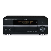
Front panel layout and controls for RX-V1800 U, C models.
Front panel layout and controls for RX-V1800 R, T, K, A, B, G, E, L models.
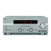
Front panel layout and controls for HTR-6190 C model.
Front panel layout and controls for HTR-6190 G model.
Front panel layout and controls for DSP-AX1800 J model.
Rear panel connections and layout for RX-V1800 U, C models.
Rear panel connections and layout for RX-V1800 R model.
Rear panel connections and layout for RX-V1800 T model.
Rear panel connections and layout for RX-V1800 K model.
Rear panel connections and layout for RX-V1800 A model.
Rear panel connections and layout for RX-V1800 B model.
Rear panel connections and layout for RX-V1800 G, E models.
Rear panel connections and layout for RX-V1800 L model.
Rear panel connections and layout for HTR-6190 C model.
Rear panel connections and layout for HTR-6190 G model.
Rear panel connections and layout for DSP-AX1800 J model.
Layout and functions of the RAV367 remote control.
Layout and functions of the RAV368 remote control.
Layout and functions of the RAV29 remote control.
Layout and functions of the RAV30 remote control.
Detailed audio specifications including power output, frequency response, and noise ratio.
Specifications for high-pass and low-pass filters used in speaker management.
Specifications for video signal types, levels, and noise ratio.
Frequency response for monitor outputs with video conversion off.
Specifications for the FM tuner section, including tuning range and sensitivity.
Specifications for the AM tuner section, including tuning range and sensitivity.
General specifications like power supply, consumption, dimensions, and finish.
Physical dimensions of the unit including width, height, and depth.
Diagram showing internal components from the top.
Diagram showing internal components from the front.
Diagram showing internal components from the rear.
Step-by-step instructions for removing the top cover.
Step-by-step instructions for removing the front panel.
Step-by-step instructions for removing the sub-chassis unit.
Procedures for checking the FL P.C.B., including grounding and cable connections.
Step-by-step instructions for removing the D-VIDEO P.C.B.
Step-by-step instructions for removing the A-VIDEO P.C.B.
Procedures for checking D-VIDEO and A-VIDEO P.C.B.s, including grounding.
Step-by-step instructions for removing the rear unit.
Procedures for checking DSP P.C.B., including grounding and cable connections.
Step-by-step instructions for removing the amplifier unit.
Procedures for checking the amplifier unit, including grounding and cable connections.
Instructions on updating firmware using a firmware CD and required tools.
Instructions on updating firmware via PC using RS232C and required tools.
Instructions on updating firmware using USER mode.
Connection procedure for firmware update using coaxial input.
Connection procedure for firmware update using optical input.
Step-by-step procedures for firmware update using the CD.
How to confirm successful firmware update using self-diagnostic function.
Precautions and preparation steps before starting PC firmware update.
Step-by-step connection procedures for PC firmware update.
Detailed steps for writing firmware to MAIN and VIDEO sections via PC.
Steps for writing firmware to MAIN, including status confirmation.
Steps for writing firmware to VIDEO, including status confirmation.
Final steps to confirm firmware update and exit the flashing program.
Steps for writing firmware to the DSP using PC.
State of the unit when ready for writing firmware to DSP.
State of the unit during firmware writing to DSP.
How to confirm DSP firmware update status and perform final steps.
Connection and activation procedures for USER mode firmware update.
Step-by-step procedures for USER mode firmware update via CD player.
How to confirm firmware version and checksum after USER mode update.
Diagnostic check for XM Radio test tone output.
Diagnostic check for input function status.
Diagnostic check for iPod connectivity and function.
Diagnostic check for network connectivity.
Diagnostic check for USB connection status.
Diagnostic check for protection function history.
Diagnostic check for DSP P.C.B. bus connection.
Diagnostic check for D-VIDEO P.C.B. bus connection.
Diagnostic display of HDMI information.
Diagnostic selection of HDMI input ports.
Specifications for HDMI up-conversion functions.
Specifications for video signal processing modes.
Indicates menu items not applicable to these models.
Indicates menu items not applicable to these models for firmware update.
Displays model and destination information.
Software switch settings for PCB functions.
Factory preset options for memory initialization.
Displays ROM version and checksum for various components.
How to start the self-diagnostic function.
How to start self-diagnostic function with protection mode canceled.
Steps to cancel the self-diagnostic function and turn off the unit.
Displays protection history data and main menu after starting diagnostics.
Diagnostic checks for abnormal voltage in power supply section.
Diagnostic checks for abnormal DC output of power amplifier.
Diagnostic checks for excessive heat sink temperature.
How protection history is stored, cleared, and managed.
How functions are displayed on the monitor and FL display during diagnostics.
How to navigate and select main and sub-menus within diagnostics.
Additional functions available during self-diagnostic mode.
Default settings applied when starting the self-diagnostic function.
Automatic input changes that occur when selecting main menus.
Detailed explanation of the DSP THROUGH menu and its sub-menus.
Explanation of the bypass function, including analog and digital modes.
Diagram illustrating the analog bypass signal flow.
Diagram illustrating the digital bypass signal flow.
Indicates menu items not applicable to these models.
How HDMI audio signals are selected and output.
Explanation of SPDIF output.
Explanation of Multi output (DVD-AUDIO).
Explanation of DSD Direct Stream Digital output.
Explanation of DSD Direct Stream Digital output via direct mode.
How input signals are identified and speaker settings are configured.
How to select 6ch/8ch input and impedance settings.
Checking microphone input signals via A/D-D/A.
Testing and controlling amplifier power relays.
Checking FL display and image control sections, including connections.
Checking video control circuit output signals.
Outputting test noise through various channels via DSP.
Checking RS-232C data transmission and flow port.
Checking test data transmission status (OK/NG).
Displaying A/D conversion values for panel keys and protection functions.
Checking hardware flow port operation (OK/NG).
Displaying temperature detection values from thermal sensors.
Displaying total amplifier output level per channel.
Displaying limiter control values from IC402.
Displaying the output condition of amplifier power relays.
Displaying the detected model name.
Checking panel key A/D values and confirming constant of pressure resistors.
Displaying destination detection value.
Checking XM Radio antenna output.
Outputting ISO tone at specified frequencies.
Turning off power to the XM module.
Displaying status data in hexadecimal notation for input functions.
Testing the DOCK connector without the iPod.
Checking network status (IP address, MAC address).
Checking USB connection status (USB 1 track, USB 2 track).
Displaying and clearing protection history.
Diagnosing DSP P.C.B. bus connection and self-diagnosis.
Diagnosing D-VIDEO P.C.B. bus connection and self-diagnosis.
Displaying HDMI module model name.
Displaying the product ID stored in the HDMI module.
Displaying the vendor name stored in the HDMI module.
Selecting HDMI input ports for input and reproduction.
Selecting HDMI IN 3 device for input and reproduction.
Selecting HDMI IN 4 device for input and reproduction.
Converting and outputting image signals to HDMI OUT.
Explanation of the HDMI decoder block.
Indicates HDMI YGV is not applicable to these models.
Explanation of the HDMI I/P block.
Explanation of HDMI 720p up-conversion.
Explanation of HDMI 1080p up-conversion.
Explanation of HDMI SMART ZOOM up-conversion.
How image signals are converted and output.
Notes on DIGITAL THR COMP output limitations.
Explanation of DIGITAL THR CVBS conversion.
Explanation of DIGITAL THR Y/C conversion.
Explanation of DIGITAL BYPASS conversion.
Explanation of ANALOG BYPASS conversion.
Displaying test patterns for video signal verification.
Displays information about incoming image signals.
Indicates menu items not applicable to these models.
Selecting this option when writing firmware.
Displays information on the model and destination.
Switching PCB function settings via software for product activation.
Selecting between PCB or SOFT mode for software switches.
Selecting between NTSC and PAL TV formats.
Selecting AAC existence status (EXIST/NOT).
Selecting CSII existence status (EXIST/NOT).
Selecting XM existence status (EXIST/NOT).
Selecting Neural Surround status (EXIST/NOT).
Selecting RDS existence status (EXIST/NOT).
Selecting FM/AM tuning mode (10/200, 9/50, 10/100).
Selecting TMP TEST mode for J, UC, RTKA, BGE or L.
Reserving and inhibiting initialization of back-up RAM.
Option to prevent RAM initialization and protect user settings.
Option to reserve RAM initialization for factory settings.
Table listing factory preset station data for FM and AM.
Displays firmware version and checksum for MAIN, VIDEO, DSP1, DSP2, XM.
Core service and adjustment procedures for the amplifier section.
Procedure to confirm and adjust amplifier idling current.
Interface information including pin connections and grid assignments.
Pin connection diagrams for various connectors.
Grid assignment for FL display segments.
Anode connection details for various pins.
Component data including IC details and pinouts.
Details of the M30845MW microprocessor IC.
Details of the M3087BFKBGP microprocessor IC.
Component layout diagrams for various printed circuit boards.
Component layout diagram for the DSP P.C.B. (Side A).
Component layout diagram for the DSP P.C.B. (Side B).
Component layout for FUNCTION (1) P.C.B. (Side A).
Component layout for FUNCTION (1) P.C.B. (Side B).
Component layout for FUNCTION (2) P.C.B. (Side A).
Component layout for FUNCTION (2) P.C.B. (Side B).
Component layout for OPERATION (1) P.C.B. (Side A).
Component layout for OPERATION (2) P.C.B. (Side A).
Component layout for OPERATION (2) P.C.B. (Side B).
Component layout for OPERATION (4) P.C.B. (Side B).
Component layout for OPERATION (5) P.C.B. (Side B).
Component layout for OPERATION (3) P.C.B. (Side A).
Component layout for OPERATION (4) P.C.B. (Side A).
Component layout for MAIN (1) P.C.B. (Side A).
Component layout for MAIN (1) P.C.B. (Side B).
Component layout for MAIN (2) P.C.B. (Side A).
Component layout for MAIN (3) P.C.B. (Side A).
Component layout for MAIN (4) P.C.B. (Side A).
Component layout for MAIN (2) P.C.B. (Side B).
Component layout for MAIN (3) P.C.B. (Side B).
Component layout for MAIN (4) P.C.B. (Side B).
Component layout for POWER (1) P.C.B. (Side A).
Component layout for POWER (1) P.C.B. (Side B).
Component layout for POWER (2) P.C.B. (Side A).
Component layout for POWER (5) P.C.B. (Side A).
Component layout for POWER (6) P.C.B. (Side A).
Component layout for POWER (5) P.C.B. (Side B).
Component layout for POWER (3) P.C.B. (Side A).
Component layout for POWER (3) P.C.B. (Side B).
Component layout for POWER (4) P.C.B. (Side A).
Component layout for POWER (4) P.C.B. (Side B).
Component layout for A-VIDEO P.C.B. (Side A).
Component layout for A-VIDEO P.C.B. (Side B).
Component layout for D-VIDEO P.C.B. (Side A).
Component layout for D-VIDEO P.C.B. (Side B).
Component layout for FL (1) P.C.B. (Side A).
Component layout for FL (1) P.C.B. (Side B).
Component layout for FL (2) P.C.B. (Side A).
Component layout for FL (2) P.C.B. (Side B).
Component layout for FL (3) P.C.B. (Side A).
Component layout for FL (4) P.C.B. (Side A).
Component layout for FL (3) P.C.B. (Side B).
Component layout for FL (4) P.C.B. (Side B).
Component layout for FL (5) P.C.B. (Side A).
Component layout for FL (6) P.C.B. (Side A).
Component layout for FL (5) P.C.B. (Side B).
Component layout for FL (6) P.C.B. (Side B).
Pin connection diagrams for various components.
Pin connection diagrams for integrated circuits (ICs).
Pin connection diagrams for various diodes.
Pin connection diagrams for various transistors.
Circuit diagrams for various sections of the unit.
Schematic diagram section for DSP (part 1 of 3).
Schematic diagram section for DSP (part 2 of 3).
Schematic diagram section for DSP (part 3 of 3).
Schematic diagram section for FUNCTION (1).
Schematic diagram section for FUNCTION (2).
Procedures for operating various sections like OPERATION (1) to (5).
Operational procedures for OPERATION (1) section.
Operational procedures for OPERATION (2) section.
Operational procedures for OPERATION (3) section.
Operational procedures for OPERATION (4) section.
Operational procedures for OPERATION (5) section.
Schematic diagrams for MAIN (1) through MAIN (4) units.
Schematic diagram for MAIN (1) unit.
Schematic diagram for MAIN (2) unit.
Schematic diagram for MAIN (3) unit.
Schematic diagram for MAIN (4) unit.
Schematic diagrams for POWER (1) through POWER (6) units.
Schematic diagram for POWER (1) unit.
Schematic diagram for POWER (2) unit.
Schematic diagram for POWER (3) unit.
Schematic diagram for POWER (4) unit.
Schematic diagram for POWER (5) unit.
Schematic diagram for POWER (6) unit.
Schematic diagram for A-VIDEO section.
Schematic diagram for A-VIDEO (part 1 of 2).
Schematic diagram for D-VIDEO section.
Schematic diagram section for D-VIDEO (part 1 of 5).
Schematic diagram section for D-VIDEO (part 2 of 5).
Schematic diagram section for D-VIDEO (part 3 of 5).
Schematic diagram section for D-VIDEO (part 4 of 5).
Schematic diagram for FL display.
Schematic diagram for FL display (part 1 of 2).
Schematic diagram for FL display (part 2 of 2).
List of all replaceable parts for the unit.
List of electrical components with part numbers and descriptions.
Replacement parts list for the DSP P.C.B.
Replacement parts list for the FUNCTION P.C.B.
Replacement parts list for the MAIN P.C.B.
Replacement parts list for the POWER P.C.B.
Replacement parts list for POWER and A-VIDEO P.C.B.s.
Replacement parts list for the A-VIDEO P.C.B.
Replacement parts list for the D-VIDEO P.C.B.
Replacement parts list for the FL P.C.B.
Exploded view diagram showing the overall assembly.
Exploded view diagram showing the amplifier unit assembly.
List of included accessories with the unit.
List of included remote controls (RAV367, RAV368).
List of included zone remote controls (RAV29, RAV30).
List of included power cables.
List of included service tools.
Table mapping key names to their corresponding codes for different remote models.
Key codes for various source types and TV modes.
Procedures for advanced setup and system configuration.
Steps for designing and configuring the audio system.
Setting the remote control color option.
Procedures for setting up the advanced menu.
Procedures for learning functions for remote control.
Procedures for remote control learning function.
Procedures for DIY DSP settings.
Steps to enter the setup menu.