CB801
CB802
CB803
CB804
IC801
JK803
JK802
JK801
IC802
CB810
CB812
CB809
IC801
IC805
IC805
CB807
CB806
CB805
A
1
2
3
4
5
6
7
8
9
10
BCDEFGH I JK
L MN
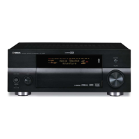
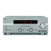
RX-V1800/HTR-6190/DSP-AX1800
126
★ All voltages are measured with a 10MΩ/V DC electronic voltmeter.
★ Components having special characteristics are marked s and must be replaced
with parts having specifications equal to those originally installed.
★ Schematic diagram is subject to change without notice.
OPERATION
0
0
2.9
2.9
5.0
5.0
5.0
0
0
0
0
0
4.3
4.3
4.3
0
10.4 9.8
9.8
0
0
-10.0
-10.6
-10.0
0
0
0
0
0
0
0.7
0.7
0
0
10.4
10.4
-10.6
0
0
0
0
0
0
0
5.0
1SS355
1SS355
PHONES
OPTIMIZER
MIC
1SS355
OPERATION (1)
OPERATION (2)
OPERATION (3)
OPERATION (5)
OPERATION (4)
VOLUME
ON/OFF
MASTER
ON/OFF
IC805: BA15218F
Dual high slew rate, low noise operational amplifier
–+
+–
1
2
3
4
8
7
6
5
OUT1
– IN1
+ IN1
V
EE
VCC
OUT2
– IN2
+ IN2
1ch
2ch
IC801: NJM4565M
Dual operational amplifier
8
2, 6
3, 5
1, 7
4
V+
–INPUT
+INPUT
V–
OUTPUT
Y4
B2
GND 3
IC802: SN74AHCT1G32DCKR
Single 2-input positive-OR gate
Vcc5A1
to DSP_W5001
Page 119
F1
to FUNCTION (2)_W301A
Page 125
D1
to FUNCTION (2)_W301B
Page 124
M3
to A-VIDEO_W2002
Writing port
Page 130
C2
to FL (2)_CB971
Page 137
K3
to FL (1)_W9004
Page 136
J6
to OPERATION (4)_CB810
J2
to FL (1)_W9002
Page 136
J4
to FL (1)_W9003
Page 136
J6
to OPERATION (3)_CB804
E8

 Loading...


