EasyManua.ls Logo

Yamaha DSP-AX559 User Manual

Yamaha DSP-AX559
116 pages
To Next Page IconTo Next Page
Page #1 background imageLoading...
Page #1 background image
SERVICE MANUAL
100997
IMPORTANT NOTICE
This manual has been provided for the use of authorized YAMAHA Retailers and their service personnel.
It has been assumed that basic service procedures inherent to the industry, and more specifically YAMAHA Products, are already
known and understood by the users, and have therefore not been restated.
WARNING: Failure to follow appropriate service and safety procedures when servicing this product may result in personal
injury, destruction of expensive components, and failure of the product to perform as specified. For these reasons,
we advise all YAMAHA product owners that any service required should be performed by an authorized
YAMAHA Retailer or the appointed service representative.
IMPORTANT: The presentation or sale of this manual to any individual or firm does not constitute authorization, certification or
recognition of any applicable technical capabilities, or establish a principle-agent relationship of any form.
The data provided is believed to be accurate and applicable to the unit(s) indicated on the cover. The research, engineering, and
service departments of YAMAHA are continually striving to improve YAMAHA products. Modifications are, therefore, inevitable
and specifications are subject to change without notice or obligation to retrofit. Should any discrepancy appear to exist, please
contact the distributor's Service Division.
WARNING: Static discharges can destroy expensive components. Discharge any static electricity your body may have
accumulated by grounding yourself to the ground buss in the unit (heavy gauge black wires connect to this buss).
IMPORTANT: Turn the unit OFF during disassembly and part replacement. Recheck all work before you apply power to the unit.
CONTENTS
TO SERVICE PERSONNEL ...................................... 2–3
FRONT PANELS ........................................................ 3–4
REAR PANELS .......................................................... 5–8
REMOTE CONTROL PANELS ...................................... 9
SPECIFICATIONS / 参考仕様 ................................ 10–12
INTERNAL VIEW ......................................................... 13
DISASSEMBLY PROCEDURES/分解手順 ......... 14–17
SELF DIAGNOSIS FUNCTION (DIAG)/
自己診断機能(ダイアグ)........................................ 18–42
AMP ADJUSTMENT/アンプ部調整 ........................... 43
DISPLAY DATA ..................................................... 44–47
IC DATA ................................................................. 48–57
PIN CONNECTION DIAGRAM .............................. 58–59
BLOCK DIAGRAMS .............................................. 61–63
PRINTED CIRCUIT BOARDS................................ 64–80
SCHEMATIC DIAGRAMS ...................................... 81–88
REPLACEMENT PARTS LIST ............................ 89–114
REMOTE CONTROL.................................................. 115
ADVANCED SETUP .................................................. 116
P.O.Box 1, Hamamatsu, Japan
AV RECEIVER/AV AMPLIFIER
RX-V559/HTR-5950/DSP-AX559
RX-V559/HTR-5950/
DSP-AX559
2006 All rights reserved.
This manual is copyrighted by YAMAHA and may not be copied or
redistributed either in print or electronically without permission.
'06.02

Table of Contents

Question and Answer IconNeed help?

Do you have a question about the Yamaha DSP-AX559 and is the answer not in the manual?

Yamaha DSP-AX559 Specifications

General IconGeneral
TypeAV Receiver
Audio Channels7.1
Signal-to-Noise Ratio100 dB
Input Sensitivity200 mV
Frequency Response10 Hz - 100 kHz
Surround SoundDolby Digital, DTS
Input Sensitivity/Impedance47 kOhms (Line)
Video ConnectionsComponent, Composite, S-Video
Audio Section192kHz/24-bit DACs for all channels
Power Output100W per channel (8 ohms, 20Hz-20kHz, 0.09% THD)

Summary

Important Notice

Service Personnel Information

Critical Components Information

Details on components requiring specific part replacements for optimal performance and safety.

Leakage Current Measurement

Procedure for verifying proper insulation of exposed conductive surfaces after service.

Chemical Content Warning

Lead Free Solder Information

Front Panel Layouts

RX-V559 (U, C models) Front Panel

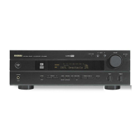
Diagram and layout for the front panel of RX-V559 (U, C) models.

RX-V559 (R, T, K, A, G, E, L models) Front Panel

Diagram and layout for the front panel of RX-V559 (R, T, K, A, G, E, L) models.

Rear Panel Layouts

RX-V559 (U, C models) Rear Panel

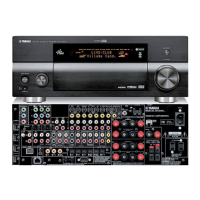
Diagram and layout for the rear panel of RX-V559 (U, C) models.

RX-V559 (R model) Rear Panel

Diagram and layout for the rear panel of RX-V559 (R) model.

RX-V559 (T model) Rear Panel

Diagram and layout for the rear panel of RX-V559 (T) model.

Remote Control Panels

RAV322 and RAV323 Remote Models

Identification of the RAV322 and RAV323 remote control units.

Remote Control Model Compatibility

Mapping of remote models to compatible receiver units.

Technical Specifications

Audio Section Specifications

Detailed specifications for the audio output, input, and processing sections.

Video Section Specifications

Detailed specifications for video signal input, output, and conversion.

FM Section Specifications

Detailed specifications for the FM tuner performance.

AM Section Specifications

Detailed specifications for the AM tuner performance.

General Specifications and Dimensions

Unit Dimensions

Physical measurements (Width x Height x Depth) of the unit.

Set Menu Table

Internal View Diagrams

RX-V559 and DSP-AX559 Internal View

Diagram showing the internal layout for RX-V559 and DSP-AX559 models.

HTR-5950 Internal View

Diagram showing the internal layout for the HTR-5950 model.

Disassembly Procedures

1. Removal of Top Cover

Step-by-step instructions for removing the unit's top cover.

2. Removal of Front Panel Unit

Step-by-step instructions for removing the front panel assembly.

3. Removal of Plate Side

Step-by-step instructions for removing the side plates.

4. Removal of Sub Chassis Unit

Step-by-step instructions for removing the sub chassis unit.

Additional Disassembly Steps

5. Removal of FUNCTION (1) P.C.B.

Instructions for removing the FUNCTION (1) printed circuit board.

6. Removal of DSP P.C.B.

Instructions for removing the DSP printed circuit board.

7. Removal of VIDEO P.C.B.

Instructions for removing the VIDEO printed circuit board.

8. Removal of FUNCTION (2) P.C.B.

Instructions for removing the FUNCTION (2) printed circuit board.

9. Removal of TUNER

Instructions for removing the TUNER unit.

10. Removal of MAIN P.C.B.s

Instructions for removing the MAIN printed circuit boards.

Printed Circuit Board (P.C.B.) Check Procedure

Self Diagnosis Function (DIAG) Guide

ANALOG BYPASS DIAG Mode

Diagnostic mode for testing analog signal bypass functionality.

DSP BYPASS DIAG Mode

Diagnostic mode for testing DSP signal bypass functionality.

RAM MARGIN DIAG Mode

Diagnostic mode for checking RAM margin.

Pro Logic DIAG Mode

Diagnostic mode for testing Pro Logic processing.

SPEAKERS SET DIAG Mode

Diagnostic mode for checking speaker settings.

MANUAL TEST DIAG Mode

Diagnostic mode for manual signal testing.

FACTORY PRESET DIAG Mode

Diagnostic mode for factory preset initialization.

AD DATA CHECK DIAG Mode

Diagnostic mode for checking Analog-to-Digital data.

VIDEO DIAG Mode

Diagnostic mode for testing video signal processing.

XM STATUS DIAG Mode

Diagnostic mode for checking XM status.

IF STATUS DIAG Mode

Diagnostic mode for checking input signal status.

DSP BUS CHECK DIAG Mode

Diagnostic mode for checking DSP bus connections.

PROTECTION HISTORY DIAG Mode

Diagnostic mode for checking protection history.

SOFTWARE VERSION DIAG Mode

Diagnostic mode for viewing software versions.

TI (DSP) BOOT DIAG Mode

Diagnostic mode for checking TI (DSP) boot status.

Starting DIAG Procedure

Starting DIAG in Protection Cancel Mode

Procedure to start DIAG with protection functions temporarily disabled.

CAUTION Regarding DIAG Mode

Canceling DIAG Procedure

DIAG Start-up Display Information

Display Without Protection History

Screen indication when no protection history is present.

Display With Protection History

Screen indication when protection history is present.

DIAG Menu Operation and Display Details

Display During Menu Operation

Describes screen and FL indicator output during DIAG menu operation.

DIAG Menu and Sub-Menu Operation

How to select and navigate through DIAG menus and sub-menus.

Functions Available in DIAG Mode

Initial Settings for DIAG Start

Details of DIAG Menu Items

1. BYPASS Menu Item Details

Explanation of the BYPASS menu item's functions.

2. RAM THROUGH Menu Item Details

Explanation of the RAM THROUGH menu item's functions.

RAM MARGIN Setting

Specific setting for RAM margin in RAM THROUGH.

RAM FULL BIT Setting

Specific setting for RAM full bit in RAM THROUGH.

3. PRO LOGIC Menu Item Details

Explanation of the PRO LOGIC menu item's functions.

4. SPEAKERS SET Menu Item Details

Explanation of the SPEAKERS SET menu item's functions.

5. XCH INPUT Menu Item Details

Explanation of the XCH INPUT menu item's functions.

6. MIC CHECK Menu Item Details

Explanation of the MIC CHECK menu item's functions.

7. DISPLAY CHECK Menu Item Details

Explanation of the DISPLAY CHECK menu item's functions.

8. MANUAL TEST Menu Item Details

Explanation of the MANUAL TEST menu item's functions.

9. FACTORY PRESET Menu Item Details

Explanation of the FACTORY PRESET menu item's functions.

10. AD DATA CHECK Menu Item Details

Explanation of the AD DATA CHECK menu item's functions.

PANEL KEY (K0/K1) Functionality

Details on the functionality and behavior of panel keys.

12. XM STATUS Menu Item Details

Explanation of the XM STATUS menu item's functions.

13. iPod Menu Item Details

Explanation of the iPod connection test menu item.

16. IF STATUS Menu Item Details

Explanation of the IF STATUS menu item's functions.

17. DSP BUS CHECK Menu Item Details

Explanation of the DSP BUS CHECK menu item's functions.

18. SWFR CUT OFF Menu Item Details

Explanation of the SWFR CUT OFF menu item's functions.

19. PROTECTION SETTING Menu Item Details

Explanation of the PROTECTION SETTING menu item's functions.

20. PROTECTION HISTORY Menu Item Details

Explanation of the PROTECTION HISTORY menu item's functions.

21. SOFT SW Menu Item Details

Explanation of the SOFT SW menu item's functions.

22. SOFTWARE VERSION Menu Item Details

Explanation of the SOFTWARE VERSION menu item's functions.

23. TI (DSP) BOOT Menu Item Details

Explanation of the TI (DSP) BOOT menu item's functions.

Amplifier Adjustment Procedures

Idling Current Confirmation for Main Board

Procedure to check and adjust idling current on the main amplifier board.

Display Data Information

Pin Connection Diagram

Diagram illustrating the pin connections for various components.

Grid Assignment Diagram

Diagram showing the assignment of display segments.

Anode Connection Data

Detailed information on anode connections for display components.

IC Data Information

IC2: Microprocessor Pin Assignments

Detailed pinout and function data for the main microprocessor IC.

IC56: Digital Audio Interface Transceiver Data

Detailed pinout and function data for the audio interface IC.

IC60: Decoder/Post Processor Data

Detailed pinout and function data for the decoder/post-processor IC.

Pin Connection Diagram

Various IC and Component Diagrams

Collection of pinout diagrams for different ICs and components.

Diodes List

Transistors List

Block Diagrams

Audio Block Diagram

High-level diagram illustrating the audio signal flow.

Video Block Diagram

High-level diagram illustrating the video signal flow.

Control and Power Block Diagram

High-level diagram of control and power management systems.

Printed Circuit Boards

DSP P.C.B. (Side A) Layout

Component layout for the DSP PCB (front view).

FUNCTION (1) P.C.B. (Side A) Layout

Component layout for the FUNCTION (1) PCB (front view).

OPERATION (1) P.C.B. (Side A) Layout

Component layout for the OPERATION (1) PCB (front view).

MAIN (1) P.C.B. (Side A) Layout

Component layout for the MAIN (1) PCB (front view).

MAIN (2) P.C.B. (Side A) Layout

Component layout for the MAIN (2) PCB (front view).

DSP P.C.B. (Side B) Layout

Component layout for the DSP PCB (back view).

FUNCTION (1) P.C.B. (Side A) Layout

Component layout for the FUNCTION (1) PCB (front view).

FUNCTION (1) P.C.B. (Side B) Layout

Component layout for the FUNCTION (1) PCB (back view).

FUNCTION (2) P.C.B. (Side A) Layout

Component layout for the FUNCTION (2) PCB (front view).

FUNCTION (3) P.C.B. (Side A) Layout

Component layout for the FUNCTION (3) PCB (front view).

FUNCTION (4) P.C.B. (Side A) Layout

Component layout for the FUNCTION (4) PCB (front view).

FUNCTION (2) P.C.B. (Side B) Layout

Component layout for the FUNCTION (2) PCB (back view).

OPERATION (1) P.C.B. (Side A) Layout

Component layout for the OPERATION (1) PCB (front view).

OPERATION (2) P.C.B. (Side A) Layout

Component layout for the OPERATION (2) PCB (front view).

OPERATION (3) P.C.B. (Side A) Layout

Component layout for the OPERATION (3) PCB (front view).

OPERATION (6) P.C.B. (Side A) Layout

Component layout for the OPERATION (6) PCB (front view).

OPERATION (1) P.C.B. (Side B) Layout

Component layout for the OPERATION (1) PCB (back view).

OPERATION (3) P.C.B. (Side B) Layout

Component layout for the OPERATION (3) PCB (back view).

OPERATION (4) P.C.B. (Side A) Layout

Component layout for the OPERATION (4) PCB (front view).

OPERATION (5) P.C.B. (Side A) Layout

Component layout for the OPERATION (5) PCB (front view).

OPERATION (4) P.C.B. (Side B) Layout

Component layout for the OPERATION (4) PCB (back view).

OPERATION (5) P.C.B. (Side B) Layout

Component layout for the OPERATION (5) PCB (back view).

OPERATION (1) P.C.B. (Side A) Layout

Component layout for the OPERATION (1) PCB (front view) for HTR-5950.

OPERATION (3) P.C.B. (Side A) Layout

Component layout for the OPERATION (3) PCB (front view) for HTR-5950.

OPERATION (6) P.C.B. (Side A) Layout

Component layout for the OPERATION (6) PCB (front view) for HTR-5950.

OPERATION (1) P.C.B. (Side B) Layout

Component layout for the OPERATION (1) PCB (back view) for HTR-5950.

OPERATION (3) P.C.B. (Side B) Layout

Component layout for the OPERATION (3) PCB (back view) for HTR-5950.

OPERATION (4) P.C.B. (Side A) Layout

Component layout for the OPERATION (4) PCB (front view) for HTR-5950.

OPERATION (4) P.C.B. (Side B) Layout

Component layout for the OPERATION (4) PCB (back view) for HTR-5950.

OPERATION (5) P.C.B. (Side A) Layout

Component layout for the OPERATION (5) PCB (front view) for HTR-5950.

OPERATION (5) P.C.B. (Side B) Layout

Component layout for the OPERATION (5) PCB (back view) for HTR-5950.

MAIN (1) P.C.B. (Side A) Layout

Component layout for the MAIN (1) PCB (front view).

MAIN (2) P.C.B. (Side A) Layout

Component layout for the MAIN (2) PCB (front view).

MAIN (4) P.C.B. (Side A) Layout

Component layout for the MAIN (4) PCB (front view).

MAIN (5) P.C.B. (Side A) Layout

Component layout for the MAIN (5) PCB (front view).

VIDEO P.C.B. (Side A) Layout

Component layout for the VIDEO PCB (front view).

VIDEO P.C.B. (Side B) Layout

Component layout for the VIDEO PCB (back view).

Schematic Diagrams

DSP Schematic Diagram (1/3)

Part 1 of the DSP section schematic diagram.

DSP Schematic Diagram (2/3)

Part 2 of the DSP section schematic diagram.

DSP Schematic Diagram (3/3)

Part 3 of the DSP section schematic diagram.

FUNCTION Schematic Diagrams

Schematic diagrams for the FUNCTION circuits.

OPERATION Schematic Diagrams (RX-V559/DSP-AX559)

Schematic diagrams for the OPERATION circuits of specific models.

OPERATION Schematic Diagrams (HTR-5950)

Schematic diagrams for the OPERATION circuits of the HTR-5950 model.

MAIN Schematic Diagram

Schematic diagram of the main unit's circuits.

VIDEO Schematic Diagram

Schematic diagram of the video processing circuits.

Replacement Parts List

WARNING: Safety and Replacement Notes

Important safety warnings and notes regarding part replacement.

Electrical Component Parts List

Categorized list of electrical components and their part numbers.

Chip Resistors

Carbon Resistors

Overall Assembly Diagram (RX-V559/DSP-AX559)

Model Specific Assembly Views

Assembly diagrams tailored to different model variants.

Overall Assembly Diagram (HTR-5950)

Front Panel and Sub Chassis Unit Assembly

AMP UNIT Assembly

Overall Assembly Diagram (HTR-5950)

HTR-5950 Front Panel Unit Assembly

Remote Control Schematic Diagrams

RAV322 Remote Control Schematic

Circuit diagram for the RAV322 remote control.

RAV323 Remote Control Schematic

Circuit diagram for the RAV323 remote control.

Remote Control Key Layout

Advanced Setup Guide

Advanced Setup Procedures

Step-by-step instructions for performing advanced setup configurations.

Related product manuals