Do you have a question about the Yamaha REV7 and is the answer not in the manual?
Details on the REV7's input channels, level, and impedance.
Information on presets (ROM) and user memory (RAM).
Specifies MIDI channel and program number capabilities.
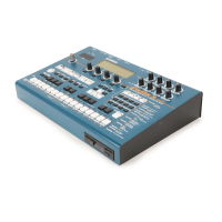
Details on display, knobs, and keys for front panel operation.
Technical specs like dynamic range, distortion, and residual noise.
Physical measurements of the unit in mm and inches.
The overall weight of the unit.
Voltage and frequency specifications for power supply.
The unit's electrical power usage.
Specifies functions controllable via remote.
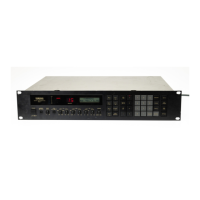
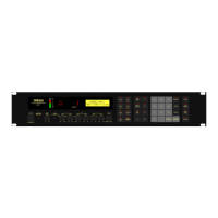
Diagram and labels for the REV7's front control panel.
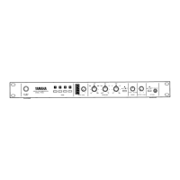
Diagram and labels for the REV7's rear panel connectors.
Diagram and labels for the REV7's remote control unit.
Detailed explanations of each programmable parameter for REV7 effects.
Time delay between direct sound and first early reflection.
Delay time for the first reflection.
Level of the first reflection relative to direct signal.
Rate at which reflected sounds decay, simulating room liveliness.
Parameter indicating time gaps between early reflections.
Rate of increase in complexity of reflections.
Selectable modes (Small Hall, Large Hall, Random, etc.) for E/R.
Additional delay time affecting both output channels.
Delay time for the first reflection.
Level of the first reflection relative to direct signal.
Independent delay time setting for the left channel.
Independent delay time setting for the right channel.
Simultaneous setting of left/right delay level.
Additional delay time affecting both output channels.
Delay time for the first reflection.
Level of the first reflection relative to direct signal.
Independent delay time setting for the left channel.
Independent delay time setting for the right channel.
Adjusts number of echoes, controlling decay time.
Low-pass filter reduces high frequencies in echoes.
Flange effect with delay time modulated by LFO.
Stereo Flange variant with REVERB TIME instead of FEEDBACK GAIN.
Modulation of amplitude and delay time by LFO for chorus.
Additional delay time before phasing effect appears.
Delay time for the first reflection.
Level of the first reflection relative to direct signal.
Basic delay time for the phasing effect.
Amount LFO varies the delay time.
Speed of LFO modulating delay time.
Block diagram of the REV7's analog signal processing path.
Block diagram of the REV7's digital signal processing path.
Description of the analog input and signal conversion stages.
Description of the digital-to-analog output stages.
Description of the mixing amplifier for direct and reverb signals.
Description of the output stage and connectors.
Description of the circuit driving the LED level meters.
Description of the muting circuit to prevent pop noise.
Overview of the digital processing components.
Description of MIDI and remote control interface circuits.
Description of the system clock timing generator.
Description of the CPU, ROM, and RAM functions.
Description of front panel control and display interfaces.
Description of the DSP, MOD, and DRAM components.
Explanation of the MIDI interface and its functions.
Location and function of adjustment potentiometers on circuit boards.
Initial settings and test equipment setup for checks.
Procedures for checking unit functions like gain and response.
Verification of the muting circuit operation.
Check of the mute switch function for reverb effects.
Procedures for calibrating various unit parameters.
Adjustment of power supply voltages and important notes.
General safety and handling precautions for servicing.
Instructions on how to access and run diagnostic tests.
Layout and identification of components on the AD circuit board.
Layout and identification of components on the EQ circuit board.
Layout and identification of components on the MT circuit board.
Layout and identification of components on the CN circuit board.
Layout and identification of components on the KY circuit board.
Layout and identification of components on the power supply board.
Schematic diagram of the REV7's analog signal path.
Schematic diagram of the REV7's digital signal path.
Pin assignments and functions for the YM3804 DSP IC.
Pin assignments and functions for the YM3807 MOD IC.
Pin assignments and functions for the MB81416 DRAM IC.
Diagram showing the exploded view of the unit's assembly.
| Type | Digital Reverb |
|---|---|
| Input Impedance | 10 kOhms |
| Output Impedance | 600 Ohms |
| Sampling Frequency | 31.25 kHz |
| A/D Conversion | 16-bit linear |
| D/A Conversion | 16-bit linear |
| Total Harmonic Distortion | Less than 0.1% |
| Memory | 30 user programs |
| Dimensions | 480 x 350 mm |
| Reverb Algorithms | Hall, Room, Plate |
| Input Level | +4 dBm |
| Output Level | +4 dBm |
| Power Consumption | 30W |
| Frequency Response | 20Hz - 20kHz |