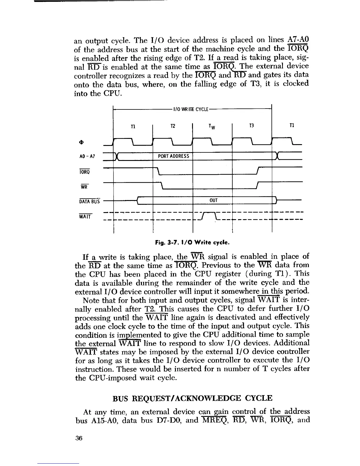
an output cycle. The I/O device address is placed on lines A7-AO
of the address bus at the start of the machine cycle and the IORQ
is enabled after the rising edge of T2. If a read is taking place, sig-
nal RD is enabled at the same time as IORQ. The external device
controller recognizes a read by the IO i and RD and gates its data
onto the data bus, where, on the falling edge of T3, it is clocked
into the CPU.
WR
T1
I/O WRITE CYCLE
T2
TW
T3 I T1
PORT ADDRESS
OUT
DATA BUS
WAIT
Fig. 3
-
7. I/O Write cycle.
If a write is taking place, the WR signal is enabled in place of
the RD at the same time as IORQ. Previous to the VVI data from
the CPU has been placed in the CPU register (during TI). This
data is available during the remainder of the write cycle and the
external I/O device controller will input it somewhere in this period.
Note that for both input and output cycles, signal WAIT is inter-
nally enabled after T2. This causes the CPU to defer further I/O
processing until the WAIT line again is deactivated and effectively
adds one clock cycle to the time of the input and output cycle. This
condition is implemented to give the CPU additional time to sample
the external WAIT line to respond to slow I/O devices. Additional
WAIT states may be imposed by the external I/O device controller
for as long as it takes the I/O device controller to execute the I/O
instruction. These would be inserted for n number of T cycles after
the CPU-imposed wait cycle.
BUS REQUEST/ACKNOWLEDGE CYCLE
At any time, an external device can gain control of the address
bus A15-AO, data bus D7-DO, and MREQ, RD, WR, IOR , and
1__^
36
 Loading...