We'll be using the internal charge pump
so connect VDD and VBAT together
(they will connect to 3.3V). GND goes to
ground.
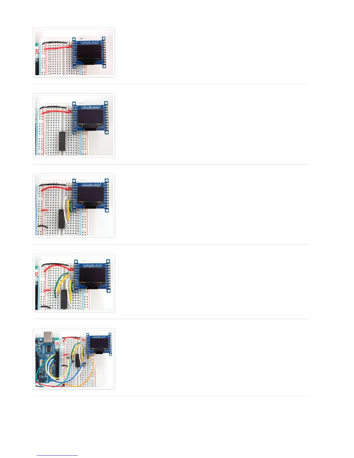
Place a CD4050 level shifter chip so pin
one is at the top.
Connect pin 10 to D/C pin 12 to CLK (SPI
clock) and pin 15 to DAT (SPI data).
Connect pin 2 to RES (reset) and pin 4
to CS (chip select). Pin 1 goes to 3.3V
and pin 8 to ground.
(Note: If using the display with other
SPI devices, D/C, CLK and DAT may be
shared, but CS must be unique for each
device.)
You can connect the inputs of the level
shifter to any pins you want but in this
case we connected digital I/O 13 to pin 3
of the level shifter, 12 to pin 5, 11 to pin
9, 10 to pin 11 and 9 to pin 14. This
matches the example code we have
written. Once you get this working, you
can try another set of pins.