EasyManua.ls Logo

Alinco DR-130 - Service Manual

Alinco DR-130
38 pages
Print Icon
To Next Page IconTo Next Page
Loading...
DR-130
Service Manual
CONTENTS
SPECIFICATIONS
1)
General
2
PARTS LAST
2)
Transmitter
2
MAIN Unit
3)
Receiver
2
CPU Unit
CIRCUIT DESCRIPTION
VCO Unit
1)
Receiver System
3
SP Unit
2)
Transmitter System
4
EJ19u.
3)
PLL Circuit
4
Mechanical Parts
4)
Terminal Function of Microprocessor
5 - 7
Others
5)
Terminal Connection of Microprocessor
8
Packing..
SEMICONDUCTOR DATA
EJ20u
1)
AK2341
9
EMS-5A
2)
AN78LO5M
10
EMS-11
3)
AN8010M
10
ADJUSTMENT
4)
BU4052BF
10
1) Required Test Equipment.
5)
LR408721
11
2) Adjustment for DR-130
6)
M5218FP
11
3) Adjustment Points
7)
M56760FP
12
4) Adjustment Quick Reference
8)
MC7808CT
13
CIRCUIT DIAGRAM
9)
RH5VA32AA-T1
13
1) EMS-5A
10)
RH5VA45AA-T1
13
2) EMS-11
11)
S-AV17
14
3) Main Unit (T/E/EZ/EA/TA)
12)
TK10487MTR
15
4) Main Unit (TEl1/TE2)
13)
AT24CO2N-10SI-2.7
15
5) CPU Unit
14)
AT24CO8-10SI-2.7
15
PC BOARD VIEW
15)
uPC1241H
16
1) Main Unit Side A
16)
Transistor, Diode and LED Outline Drawings
16
2) Main Unit Side B
17)
LCD Connection
17
3) CPU Unit Side A.
EXPLODED VIEW
4) CPU Unit Side B
1)
Bottom View
18
5) VCO Unit Side A
2)
LCD View
18
6) VCO Unit Side B
3)
Top, Front View 1
19
BLOCK DIAGRAM
4)
Top, Front View 2
20
VERSION TABLE
21
ALINCO INCORPORATED
TWIN 21 M.I.D. TOWER BUILDING 23F, 1-61, 2-CHOME,
SHIROMI CHUO-KU , OSAKA, 540-8580 JAPAN
Tel (81)6-6946-8150 fax (81)6-6946-8175
e-mail: export@alinco.co.jp
Question and Answer IconNeed help?

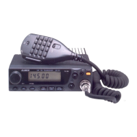
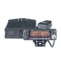
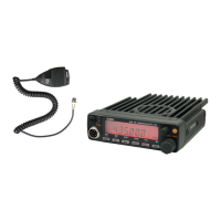
Do you have a question about the Alinco DR-130 and is the answer not in the manual?

Summary

SPECIFICATIONS

General Specifications

Details frequency coverage, resolution, impedance, power supply, dimensions, and weight.

Transmitter Specifications

Covers output power, emission mode, modulation system, deviation, and spurious emissions.

Receiver Specifications

Details receiving system, intermediate frequency, sensitivity, selectivity, and audio output.

CIRCUIT DESCRIPTION

Receiver System Circuitry

Explains the function of receiver's front-end, mixer, and IF circuits.

Transmitter System Circuitry

Describes the modulation, TX amplifier, PA circuit, and ALC circuit functions.

PLL Circuit Description

Details the VCO and PLL synthesizer circuit design and operation.

Microprocessor Terminal Functions

Lists and describes the function of each pin on the microprocessor.

Microprocessor Terminal Connections

Provides a pinout diagram showing microprocessor terminal connections.

SEMICONDUCTOR DATA

AK2341 CTCSS Encoder;Decoder Data

Datasheet for AK2341 IC, including pinout and block diagram.

AN78 L05 M Voltage Regulator Data

Datasheet for AN78L05M 5V regulator, including test circuit.

AN8010 M Voltage Regulator Data

Datasheet for AN8010M regulator, including test circuit.

BU4052 BF Analog Multiplexer Data

Datasheet for BU4052BF analog multiplexer, with function table and block diagram.

LR408721 Tone Dialer Data

Datasheet for LR408721 tone dialer, with pinout and test circuit.

M5218 FP Dual Operational Amplifiers Data

Datasheet for M5218FP dual op-amp, showing pinout.

M56760 FP Frequency Synthesizer Data

Datasheet for M56760FP frequency synthesizer, with pinout and block diagram.

MC7808 CT Voltage Regulator Data

Datasheet for MC7808CT 8V regulator, including test circuit.

RH5 VA32 AA-T1 Voltage Detector Data

Datasheet for RH5VA32AA-T1 voltage detector, showing equivalent circuit.

RH5 VA45 AA-T1 Voltage Detector Data

Datasheet for RH5VA45AA-T1 voltage detector, showing equivalent circuit.

S-AV17 RF Power Module Data

Datasheet for S-AV17 RF power module, including performance graphs.

TK10487 MTR FM IF IC Data

Datasheet for TK10487MTR FM IF IC, with specifications.

AT24 C02 N EEPROM Data

Datasheet for AT24C02N EEPROM, including pin names.

AT24 C08 EEPROM Data

Datasheet for AT24C08 EEPROM, including pin names.

μPC1241 H Audio Power Amplifiers Data

Datasheet for μPC1241H audio amplifier, including test circuit.

Component Outline Drawings

Provides outline drawings for transistors, diodes, and LEDs.

LCD Connection Details

Details the connection pinout for the LCD display module.

EXPLODED VIEW

Bottom View Assembly

Shows exploded view of bottom assembly, indicating screw locations.

LCD Module Assembly

Illustrates the assembly of the LCD module and its components.

Top Front View 1 Assembly

Displays exploded view of top/front assembly, showing component placement.

Top Front View 2 Assembly

Provides exploded view of top/front assembly, detailing parts.

VERSION TABLE

CPU UNIT Component Variations

Lists component variations for CPU unit across different radio versions.

MAIN UNIT Component Variations

Details component variations for the main unit for different radio versions.

VCO UNIT Component Variations

Specifies component variations for the VCO unit across different radio versions.

ADJUSTMENT PROCEDURES

Required Test Equipment

Lists the necessary test equipment for performing adjustments and calibrations.

DR130 Calibration Steps

Provides step-by-step procedures for adjusting the DR130 radio.

Transmitter Adjustments

Details procedures for adjusting transmitter power, deviation, and gain.

Adjustment Points Locations

Illustrates the locations of adjustment points on the circuit board.

Adjustment Quick Reference

Summarizes key adjustment parameters and their required values.

CIRCUIT DIAGRAMS

Overall Schematic Diagrams

Presents the overall schematic diagrams for the radio's circuitry.

Main Unit Circuit Diagram (T;E;EZ;EA;TA)

Shows detailed circuit diagram for Main Unit, specific to T/E/EZ/EA/TA versions.

Main Unit Circuit Diagram (TE1;TE2)

Displays circuit diagram for Main Unit, specific to TE1/TE2 versions.

CPU Unit Circuit Diagram

Provides circuit diagram for the CPU Unit, detailing its components and connections.

PC BOARD VIEWS

Main Unit PCB Layout - Side A

Illustrates component layout on Side A of the Main Unit PCB.

Main Unit PCB Layout - Side B

Shows component layout on Side B of the Main Unit PCB.

CPU Unit PCB Layout - Side A

Depicts component placement on Side A of the CPU Unit PCB.

CPU Unit PCB Layout - Side B

Shows component layout on Side B of the CPU Unit PCB.

VCO Unit PCB Layout - Side A

Illustrates component layout on Side A of the VCO Unit PCB.

VCO Unit PCB Layout - Side B

Shows component layout on Side B of the VCO Unit PCB.

BLOCK DIAGRAM

Alinco DR-130 Specifications

General IconGeneral
BrandAlinco
ModelDR-130
CategoryRadio
LanguageEnglish

Related product manuals