1–8 Reference Manual Altera Corporation
Cyclone II FPGA Starter Development Board October 2006
Introduction
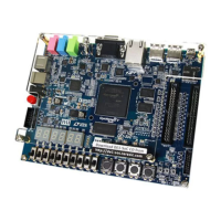
■ FineLine BGA 484-pin package
Serial Configuration Device and USB Blaster Circuit
■ Altera EPCS4 serial configuration device
■ On-board USB-Blaster chip set for programming
and user API control
■ Selectable JTAG and AS programming modes
SRAM
■ 512-KByte static RAM memory chip
■ Organized as 256K x 16 bits
■ Accessible as memory for the Nios II processor
and by the Control Panel GUI
SDRAM
■ 8-MByte single data rate synchronous dynamic RAM memory chip
■ Organized as 1M x 16 bits x 4 banks
■ Accessible as memory for the Nios II processor
and by the Control Panel GUI
Flash Memory
■ 4-MByte NOR flash memory
■ 8-bit data bus
■ Accessible as memory for the Nios II processor
and by the Control Panel GUI
SD Card Socket
■ Provides SPI mode for SD card access
■ Accessible as memory for the Nios II processor
with the DE1 SD Card Driver
Push Button Switches
■ 4 push button switches
■ Debounced by a Schmitt trigger circuit
■ Normally HIGH; generates one active-LOW pulse
when the switch is pressed
Toggle Switches
■ 10 toggle switches for user inputs


 To Next Page