2–14 Reference Manual Altera Corporation
Cyclone II FPGA Starter Development Board October 2006
Development Board Components
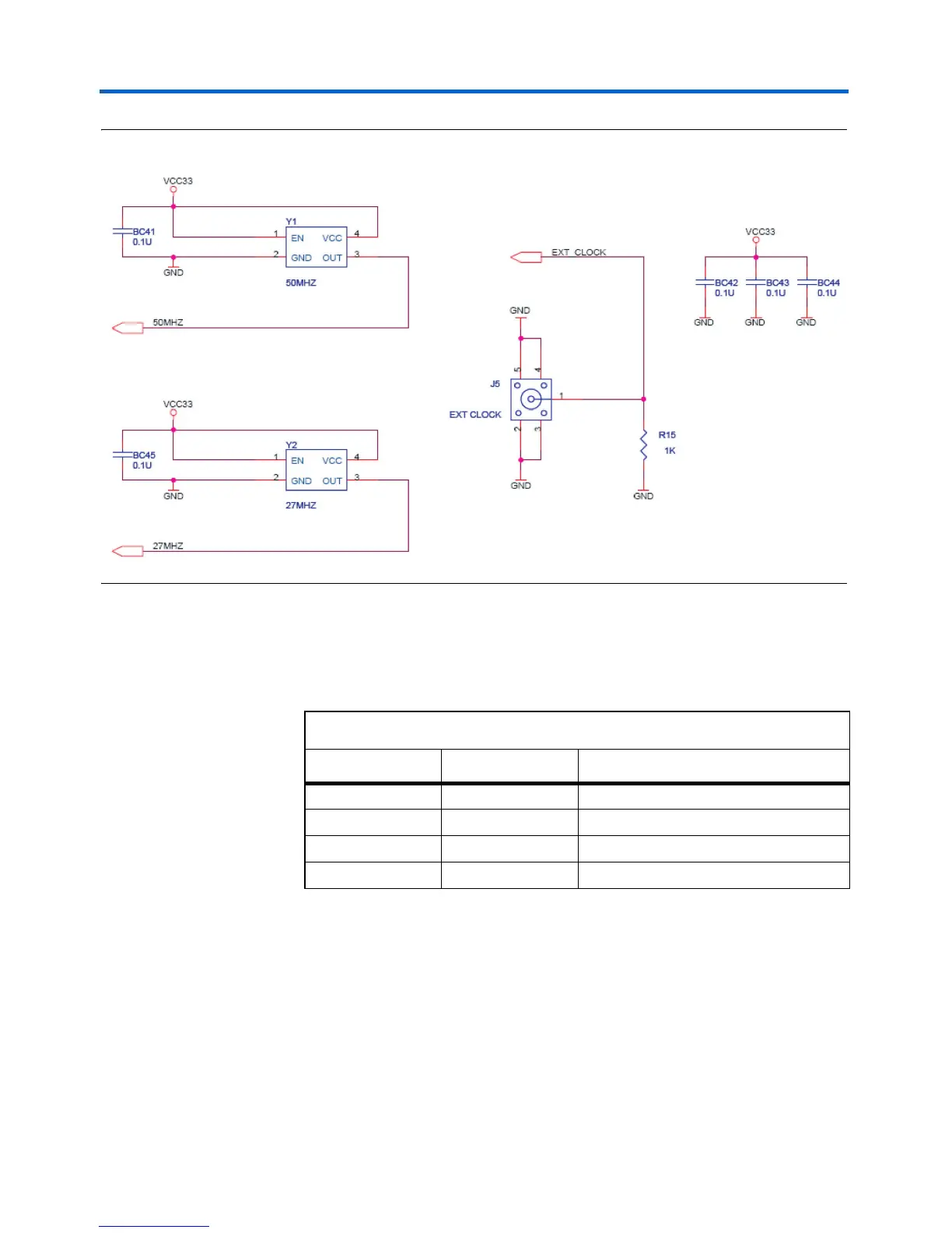
Figure 2–7. Clocking Circuit Schematic Diagram
Clock Input Pin List
Table 2–9 lists the FPGA pins assigned to the display segments.
Switches
The development board provides the following user switches:
■ Power ON/OFF switch
■ RUN/PROG switch
■ 4 push button switches
■ 10 Toggle switches
Table 2–9. Clock Circuit FPGA Pin Connections
Signal Name FPGA Pin Description
CLOCK_27 PIN_D12 27 MHz clock input
CLOCK_50 PIN_L1 50 MHz clock input
CLOCK_24 PIN_B12 24 MHz clock input from USB Blaster
EXT_CLOCK PIN_M21 External (SMA) clock input