2–8 Reference Manual Altera Corporation
Cyclone II FPGA Starter Development Board October 2006
Development Board Components
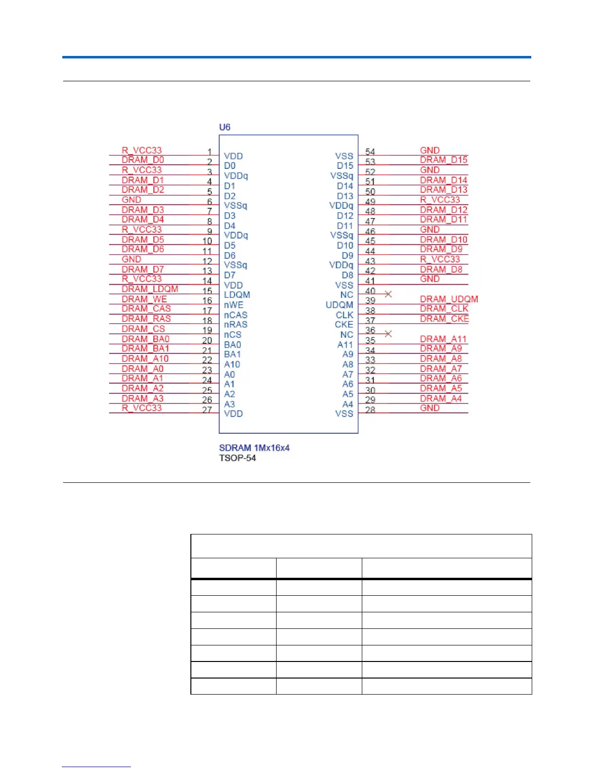
Figure 2–4. SDRAM Interface Connections Diagram
Table 2–6 lists the FPGA pins assigned to the SDRAM.
Table 2–6. SDRAM FPGA Pin Connections (Part 1 of 2)
Signal Name FPGA Pin Description
DRAM_ADDR[0] PIN_W4 SDRAM Address[0]
DRAM_ADDR[1] PIN_W5 SDRAM Address[1]
DRAM_ADDR[2] PIN_Y3 SDRAM Address[2]
DRAM_ADDR[3] PIN_Y4 SDRAM Address[3]
DRAM_ADDR[4] PIN_R6 SDRAM Address[4]
DRAM_ADDR[5] PIN_R5 SDRAM Address[5]
DRAM_ADDR[6] PIN_P6 SDRAM Address[6]