2–12 Reference Manual Altera Corporation
Cyclone II FPGA Starter Development Board October 2006
Development Board Components
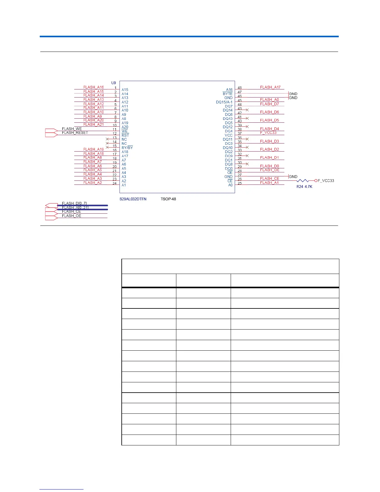
Figure 2–6. Flash Memory Interface Connections Diagram
Table 2–8 lists the FPGA pins assigned to the flash memory.
Table 2–8. Flash Memory FPGA Pin Connections (Part 1 of 2)
Signal Name FPGA Pin Description
FL_ADDR[0] PIN_AB20 FLASH Address[0]
FL_ADDR[1] PIN_AA14 FLASH Address[1]
FL_ADDR[2] PIN_Y16 FLASH Address[2]
FL_ADDR[3] PIN_R15 FLASH Address[3]
FL_ADDR[4] PIN_T15 FLASH Address[4]
FL_ADDR[5] PIN_U15 FLASH Address[5]
FL_ADDR[6] PIN_V15 FLASH Address[6]
FL_ADDR[7] PIN_W15 FLASH Address[7]
FL_ADDR[8] PIN_R14 FLASH Address[8]
FL_ADDR[9] PIN_Y13 FLASH Address[9]
FL_ADDR[10] PIN_R12 FLASH Address[10]
FL_ADDR[11] PIN_T12 FLASH Address[11]
FL_ADDR[12] PIN_AB14 FLASH Address[12]
FL_ADDR[13] PIN_AA13 FLASH Address[13]
FL_ADDR[14] PIN_AB13 FLASH Address[14]