DE1-SOC COMPUTER SYSTEM WITH NIOS II For Quartus II 15.0
Expansion
ports
Cyclone V
FPGA
PS/2
ports
Timers
SW
9-0
LEDR
9-0
Parallel
ports
Parallel
ports
HEX5-HEX0
7-Segment
KEY
3-0
SDRAM
port
SDRAM
chip
IrDA
On-chip
memory
Video-in
port
TV
Decoder
Host computer
USB
Blaster
VGA
DAC
Audio
CODEC
Video-out
port
Audio
port
Peripherals
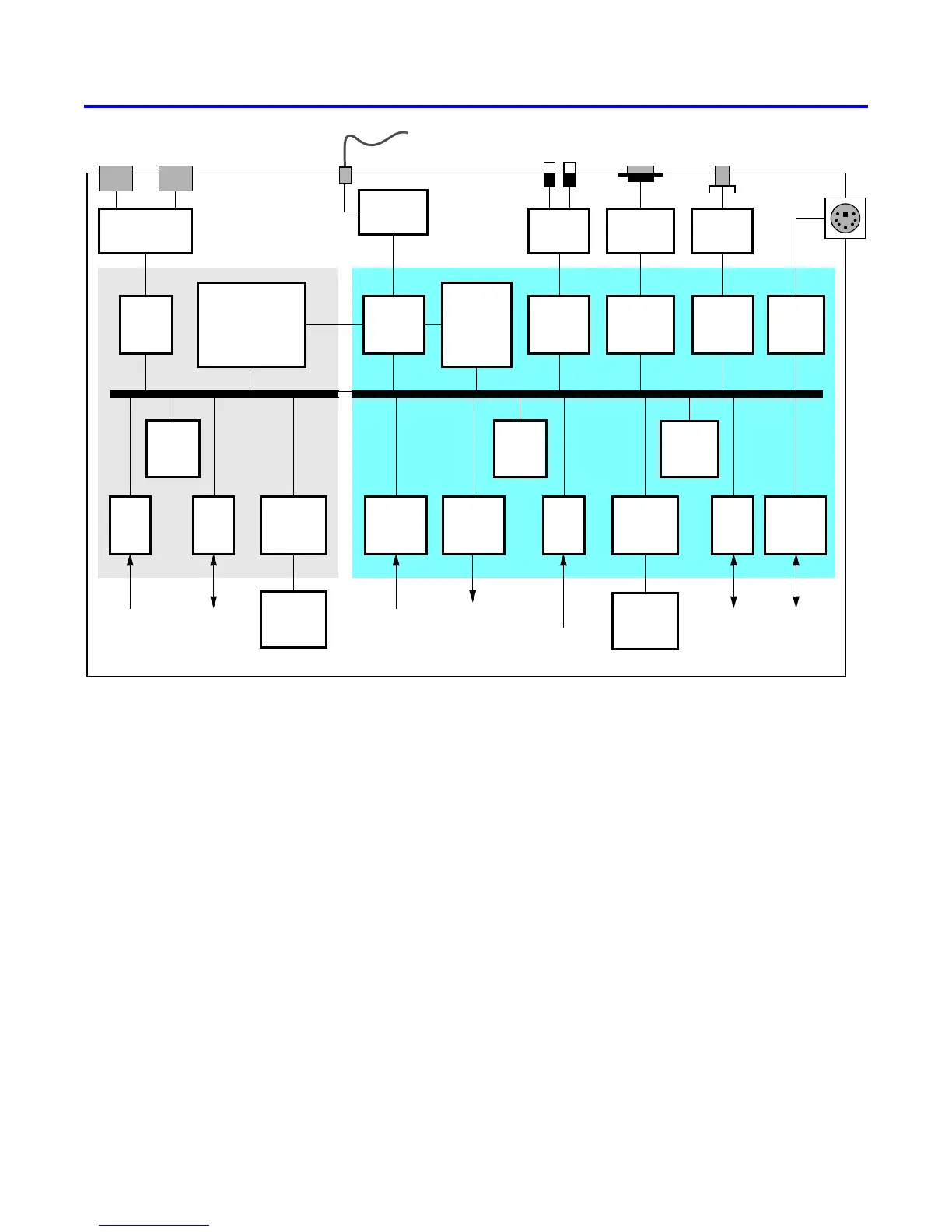
DE1-SoC
DDR3
port
DDR3
chips
Port
JTAG
ports
Parallel
ports
ARM
MPCore
Cortex A9
Timers
Cyclone V
HPS
Ports
. . .
Board
Nios II
FPGA Bridges
LEDG
Port
KEY
ADC
Port
(2)
G-Sensor
Port
Figure 1. Block diagram of the DE1-SoC Computer.
edit) the contents of processor registers, display/edit the contents of memory on the DE1-SoC board, and similar
operations. The Monitor Program includes the DE1-SoC Computer as a predesigned system that can be downloaded
onto the DE1-SoC board, as well as several sample programs in assembly language and C that show how to use
the DE1-SoC Computer’s peripherals. Some images that show how the DE1-SoC Computer is integrated with the
Monitor Program are described in Section 8. An overview of the Monitor Program is available in the document
Altera Monitor Program Tutorial, which is provided in the University Program web site.
All of the I/O peripherals in the DE1-SoC Computer are accessible by the processor as memory mapped devices,
using the address ranges that are given in the following subsections.
2.3 Memory Components
The DE1-SoC Computer has DDR3 and SDRAM ports, as well as two memory modules implemented using the
on-chip memory inside the FPGA. These memories are described below.
2 Altera Corporation - University Program
2015