DE1-SOC COMPUTER SYSTEM WITH NIOS II For Quartus II 15.0
2.3.1 SDRAM
An SDRAM Controller in the FPGA provides an interface to the 64 MB synchronous dynamic RAM (SDRAM)
on the DE1-SoC board, which is organized as 32M x 16 bits. It is accessible by the Nios II processor using word
(32-bit), halfword (16-bit), or byte operations, and is mapped to the address space 0x00000000 to 0x03FFFFFF.
2.3.2 DDR3 Memory
The DE1-SoC Computer includes a 1 GB DDR3 memory that is connected to the HPS part of the Cyclone V SoC
chip. The memory is organized as 256M x 32-bits, and is accessible using word accesses (32 bits), halfwords, and
bytes. The Nios II processor can access the DDR3 memory through the FPGA bridge, using the addresses space
0x40000000 to 0x7FFFFFFF.
2.3.3 On-Chip Memory
The DE1-SoC Computer includes a 256-Kbyte memory that is implemented inside the FPGA. This memory is
organized as 64K x 32 bits, and spans addresses in the range 0x08000000 to 0x0803FFFF. The memory is used
as a pixel buffer for the video-out and video-in ports.
2.3.4 On-Chip Memory Character Buffer
The DE1-SoC Computer includes an 8-Kbyte memory implemented inside the FPGA that is used as a character
buffer for the video-out port, which is described in Section 4.2. The character buffer memory is organized as 8K x 8
bits, and spans the address range 0x09000000 to 0x09001FFF.
2.4 Parallel Ports
There are several parallel ports implemented in the FPGA that support input, output, and bidirectional transfers of
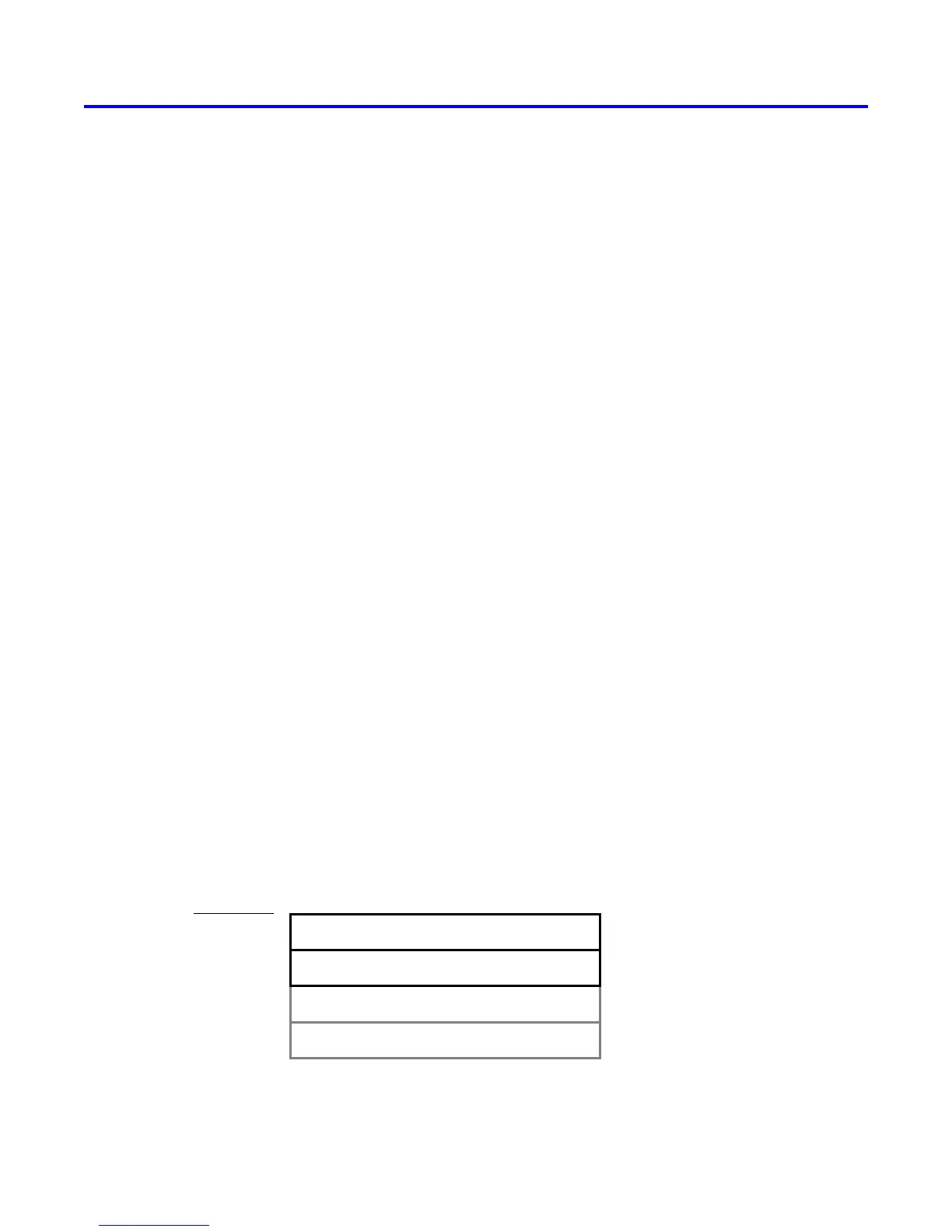
data between the Nios II processor and I/O peripherals. As illustrated in Figure 2, each parallel port is assigned
a Base address and contains up to four 32-bit registers. Ports that have output capability include a writable Data
register, and ports with input capability have a readable Data register. Bidirectional parallel ports also include a
Direction register that has the same bit-width as the Data register. Each bit in the Data register can be configured
as an input by setting the corresponding bit in the Direction register to 0, or as an output by setting this bit position
to 1. The Direction register is assigned the address Base + 4.
Address
0214331 30
. . .
Base
Base + 8
Base + C
Base + 4
Input or output data bits
Direction bits
Edge bits
Mask bits
Data register
Direction register
Interruptmask register
Edgecapture register
Direction bits
Figure 2. Parallel port registers in the DE1-SoC Computer.
Altera Corporation - University Program
2015
3
 Loading...


