DE1-SOC COMPUTER SYSTEM WITH NIOS II For Quartus II 15.0
register. If the receive FIFO overflows, then additional data is lost. When the data that is present in the receive FIFO
is available for reading, then the value of bit 15, RVALID, will be 1. Reading the character at the head of the FIFO,
which is provided in bits 7 − 0, decrements the value of RAVAIL by one and returns this decremented value as part
of the read operation. If no data is available to be read from the receive FIFO, then RVALID will be set to 0 and the
data in bits 7 − 0 is undefined.
The UART also includes a 256-character FIFO that stores data waiting to be sent to the IrDA device. Character data
is loaded into this register by performing a write to bits 7−0 of the Data register. Writing into this register has no
effect on received data. The amount of space WSPACE currently available in the transmit FIFO is provided in bits
23−16 of the Control register, as indicated in Figure 35. If the transmit FIFO is full, then any additional characters
written to the Data register will be lost.
The RE and WE bits in the Control register are used to enable Nios II processor interrupts associated with the receive
and transmit FIFOs. When enabled, interrupts are generated when RAVAIL for the receive FIFO, or WSPACE for
the transmit FIFO, exceeds 31. Pending interrupts are indicated in the Control register’s RI and WI bits, and can be
cleared by writing or reading data to/from the UART.
4.7 Analog-to-Digital Conversion Port
The Analog-to-Digital Conversion (ADC) Port provides access to the eight-channel, 12-bit analog-to-digital con-
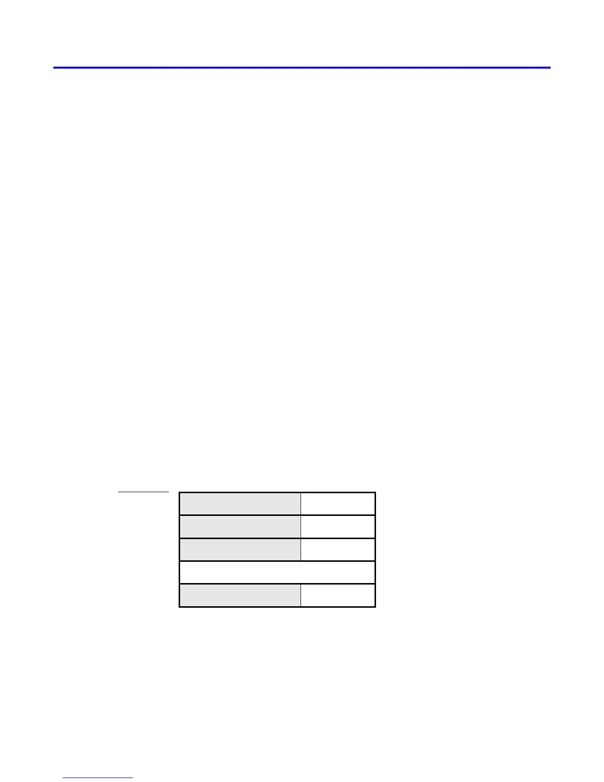
verter on the DE1-SoC board. As illustrated in Figure 36, the ADC port comprises eight 12-bit registers starting at
the base address 0xFF204000. The first two registers have dual purposes, acting as both data and control registers.
By default, the ADC port updates the A-to-D conversion results for all ports only when instructed to do so. Writing
to the control register at address 0xFF204000 causes this update to occur. Reading from the register at address
0xFF204000 provides the conversion data for channel 0. Reading from the other seven registers provides the con-
version data for the corresponding channels. It is also possible to have the ADC port continually request A-to-D
conversion data for all channels. This is done by writing the value 1 to the control register at address 0xFF204004.
Address
031
. . .
0xFF204000
0xFF20401C
0xFF204004
Unused
Channel 0 / Update
Channel 7
Channel 1 / Auto-update
... not shown
12
. . .
0xFF204008
Channel 2
11
Unused
Unused
Unused
Figure 36. ADC port registers.
Figure 37 shows the connector on the DE1-SoC board that is used with the ADC port. Analog signals in the range
of 0 V to the V
CC 5
power-supply voltage can be connected to the pins for channels 0 to 7.
Altera Corporation - University Program
2015
39
 Loading...


