DE1-SOC COMPUTER SYSTEM WITH NIOS II For Quartus II 15.0
7 Memory Layout
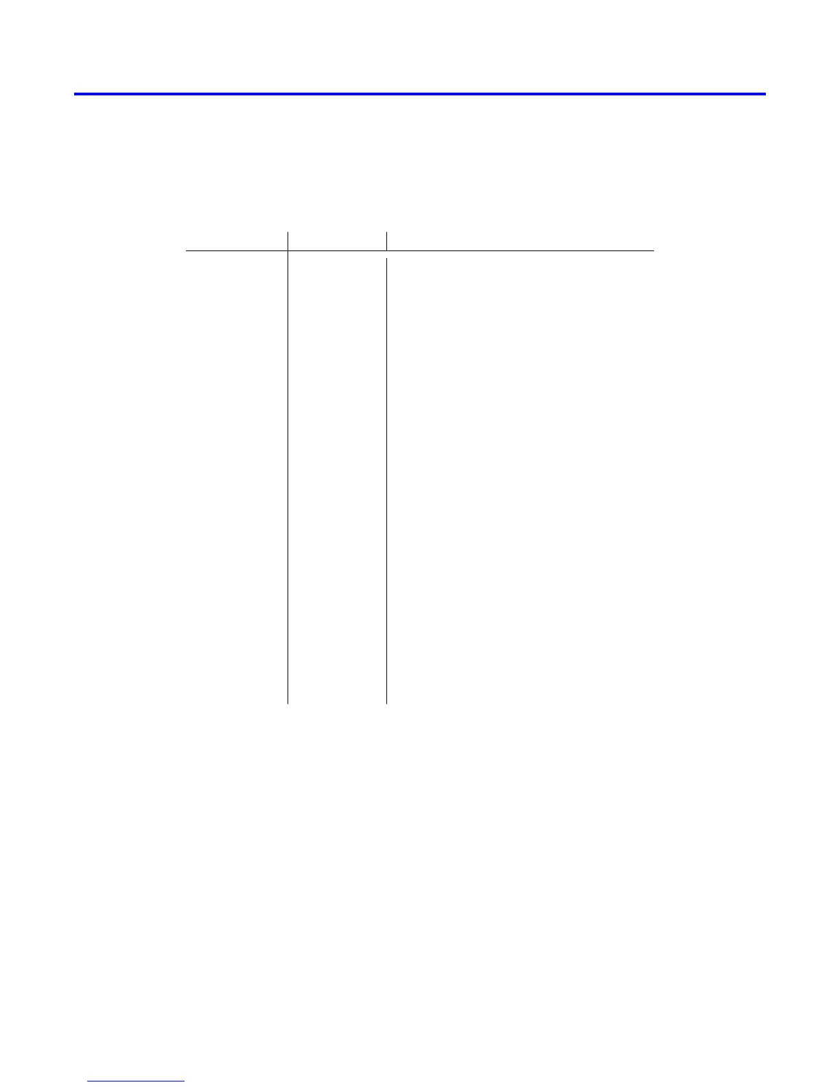
Table 2 summarizes the memory map used in the DE1-SoC Computer.
Base Address End Address I/O Peripheral
0x00000000 0x03FFFFFF SDRAM
0x08000000 0x0803FFFF FPGA On-chip Memory
0x09000000 0x09001FFF FPGA On-chip Memory Character Buffer
0x40000000 0x7FFFFFFF DDR3 Memory
0xFF200000 0xFF20000F Red LEDs
0xFF200020 0xFF20002F 7-segment HEX3−HEX0 Displays
0xFF200030 0xFF20003F 7-segment HEX5−HEX4 Displays
0xFF200040 0xFF20004F Slider Switches
0xFF200050 0xFF20005F Pushbutton KEYs
0xFF200060 0xFF20006F JP1 Expansion
0xFF200070 0xFF20007F JP2 Expansion
0xFF200100 0xFF200107 PS/2
0xFF200108 0xFF20010F PS/2 Dual
0xFF201000 0xFF201007 JTAG UART
0xFF201020 0xFF201027 Infrared (IrDA)
0xFF202000 0xFF20201F Interval Timer
0xFF202020 0xFF20202F Second Interval Timer
0xFF203000 0xFF20301F Audio/video Configuration
0xFF203020 0xFF20302F Pixel Buffer Control
0xFF203030 0xFF203037 Character Buffer Control
0xFF203040 0xFF20304F Audio
0xFF203060 0xFF203070 Video-in
0xFF204000 0xFF20401F ADC
0xFFC04000 0xFFC040FC HPS I2C0
Table 2. Memory layout used in the DE1-SoC Computer.
42 Altera Corporation - University Program
2015