Ref. Des. Feature Notes Schematic Page
U299 DDR4 DIMM CLK, 200 MHz, 3.3V LVDS,
0x09
Renesas output 2
RC21008A
93
U299 DDR4 DIMM CLK, 200 MHz, 3.3V LVDS,
0x09
Renesas output 3
RC21008A
93
U299 Adaptive SoC U1 GTYP (FMC+) CLK, 100
MHz, 3.3V LVDS, 0x09
Renesas output 6
RC21008A
93
U299 Adaptive SoC U1 GTYP (FMC+) CLK, 100
MHz, 3.3V LVDS, 0x09
Renesas output 7
RC21008A
93
U299 Adaptive SoC U1 GTYP (zSFP+) CLK,
156.25 MHz, 3.3V LVDS, 0x09
Renesas output 8
RC21008A
93
U299 Adaptive SoC U1 processing system (PS)
reference CLK, 33.33 MHz, 1.8V
LVCMOS, 0x09
Renesas output
10
RC21008A
93
U299 Master mode Ethernet CLK, 25 MHz,
1.8V LVCMOS, 0x09
Renesas output
11
RC21008A
93
U374 Adaptive SoC U1 HSDP CLK, 156.25
MHz, 3.3V LVDS
CTS
626L15625I3T
8
U344 HDMI RX RCLK, various, 3.3V differential,
0x5B
TI
TMDS1204
45
U344 HDMI RX OUT CLK, various, 3.3V
differential, 0x5B
TI
TMDS1204
45
U1 IEEE-1588 eCPRI CLK, various, 3.3V, 0x5B Adaptive SoC
XCVE2802
3, 92
The detailed device connections for the feature described in this section are
documented in the VEK280 board XDC file, referenced in Xilinx Design Constraints.
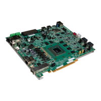
Programmable MGT RC21008A REF Clocks
[Figure 1, callout 36]