Technical Guide P92x/EN CT/E11
Modbus Protocol
MiCOM P921-P922-P923 Page 19/118
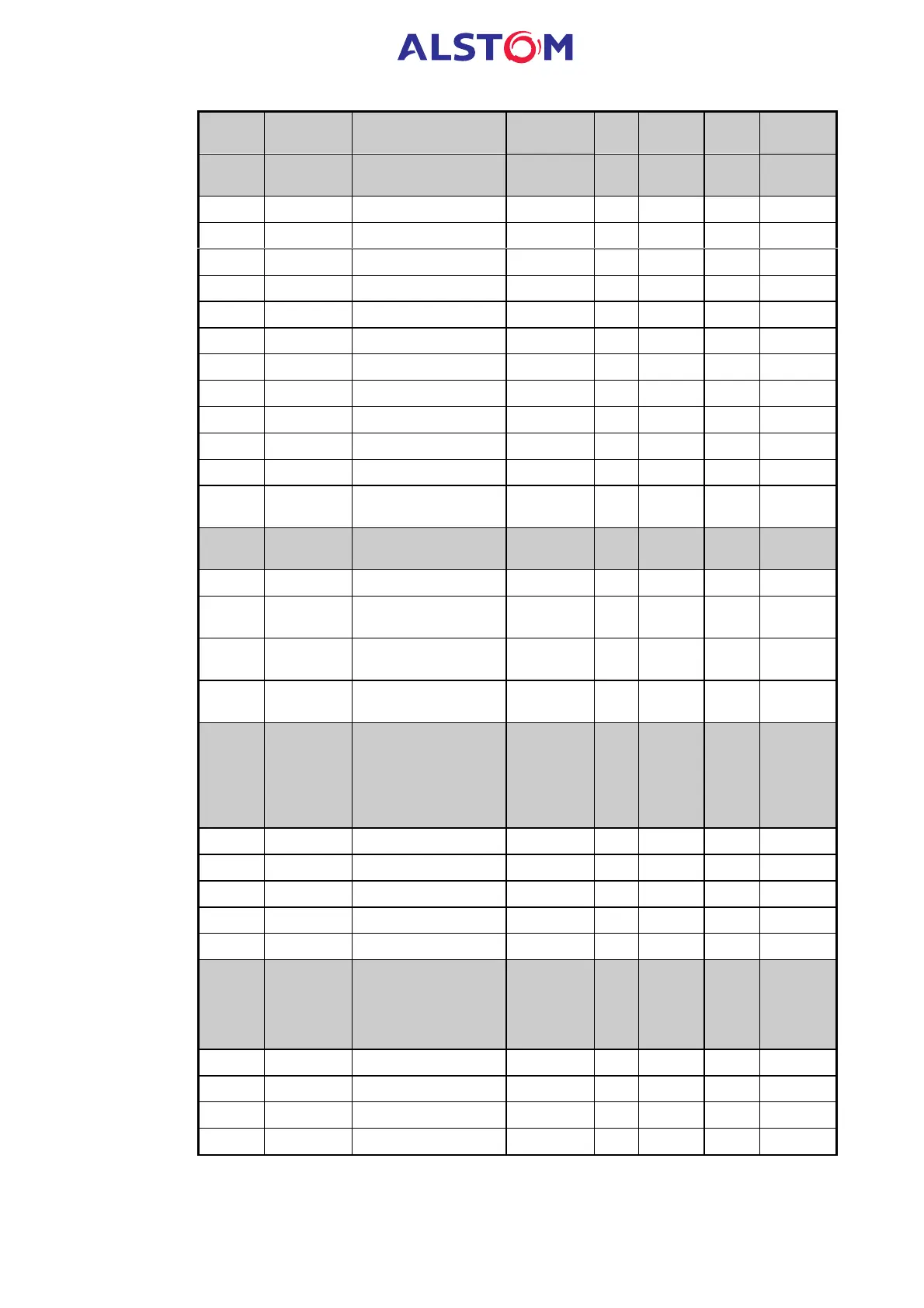
Address Group Description
Settings
range
Step Unit Format
Default
settings
0150 Leds
configuration
Led 5 1st part 1 - F19 0
0151 Led 6 1st part 1 - F19 0
0152 Led 7 1st part 1 - F19 0
0153 Led 8 1st part 1 F19 0
0154 Led 5 2nd part 1 F19' 0
0155 Led 6 2nd part 1 F19' 0
0156 Led 7 2nd part 1 F19' 0
0157 Led 8 2nd part 1 F19' 0
0158 Led 5 3rd part 1 F19'' 0
0159 Led 6 3rd part 1 F19'' 0
015A Led 7 3rd part 1 F19'' 0
015B Led 8 3rd part 1 F19'' 0
015C to
015F
Reserved
0160 Logic inputs
configuration
Logic input 1 VTA - F15 0
0161 Logic input 2 VTA - F15 0
0162 Logic input 3 (P922-
P923)
VTA - F15 0
0163 Logic input 4 (P922-
P923)
VTA - F15 0
0164 Logic input 5 (P922-
P923)
VTA - F15 0
0165 Allocation of
the protection
information to
the auxiliary
output contact
(RL2 to RL8)
df/dt1 0 to 127 1 - F14 0
0166 df/d2 0 to 127 1 - F14 0
0167 df/dt3 0 to 127 1 - F14 0
0168 df/dt4 0 to 127 1 - F14 0
0169 df/dt5 0 to 127 1 - F14 0
016A df/dt6 0 to 127 1 - F14 0
016B Allocation of
the protection
information to
the Logic
equations
df/dt1 0 to 15 1 - F54 0
016C df/dt2 0 to 15 1 - F54 0
016D df/dt3 0 to 15 1 - F54 0
016E df/dt4 0 to 15 1 - F54 0
016F df/dt5 0 to 15 1 - F54 0