57
7598H–AVR–07/09
ATtiny25/45/85
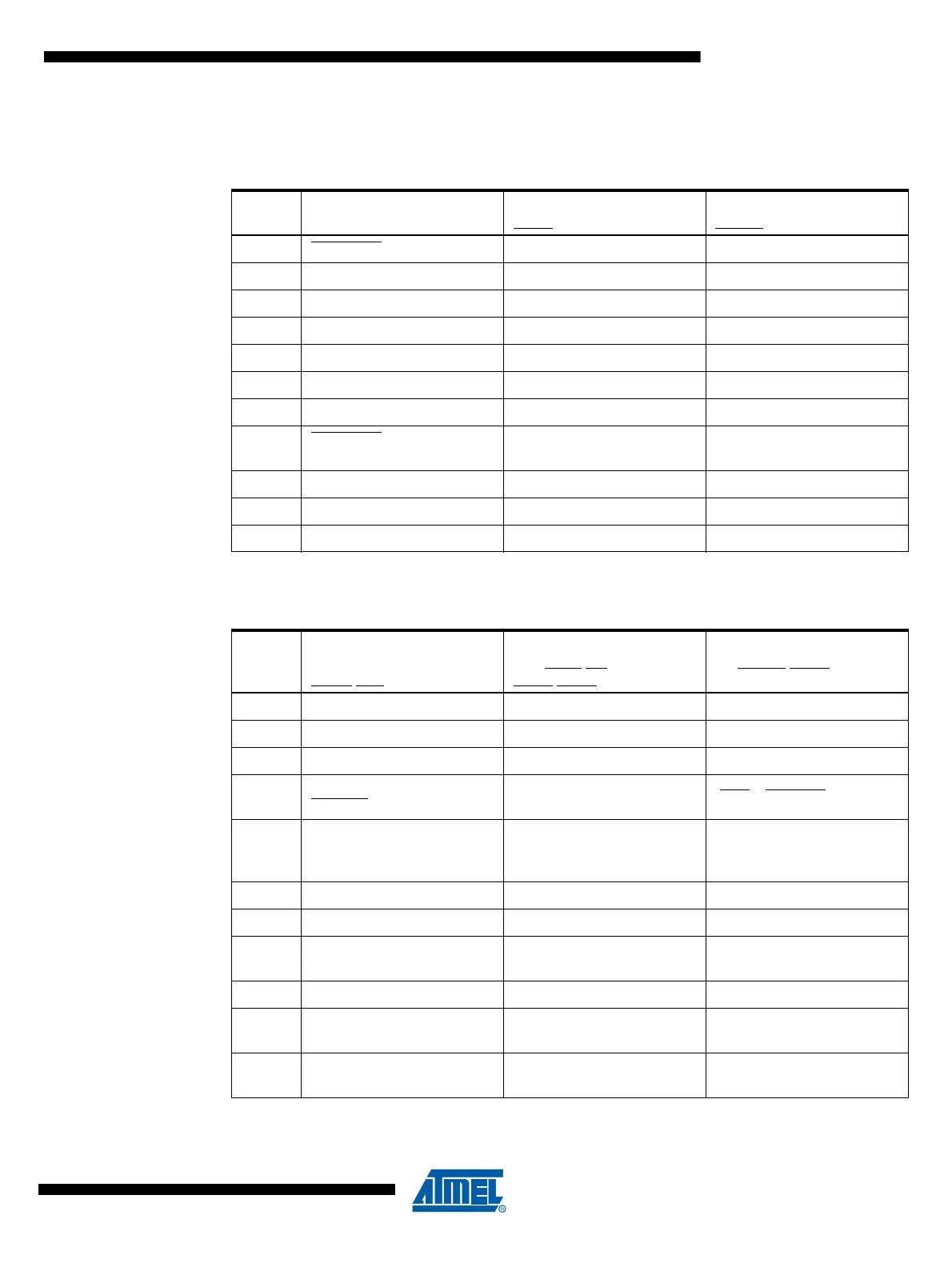
Table 10-4 and Table 10-5 relate the alternate functions of Port B to the overriding signals
shown in Figure 10-5 on page 52.
Note: 1. 1 when the Fuse is “0” (Programmed).
Table 10-4. Overriding Signals for Alternate Functions in PB5..PB3
Signal
Name
PB5/RESET/
ADC0/PCINT5
PB4/ADC2/XTAL2/
OC1B/PCINT4
PB3/ADC3/XTAL1/
_OC1B/PCINT3
PUOE RSTDISBL
(1)
• DWEN
(1)
00
PUOV100
DDOE RSTDISBL
(1)
• DWEN
(1)
00
DDOV debugWire Transmit 0 0
PVOE 0 OC1B Enable _OC1B Enable
PVOV 0 OC1B _OC1B
PTOE000
DIEOE
RSTDISBL
(1)
+ (PCINT5 •
PCIE + ADC0D)
PCINT4 • PCIE + ADC2D PCINT3 • PCIE + ADC3D
DIEOV ADC0D ADC2D ADC3D
DI PCINT5 Input PCINT4 Input PCINT3 Input
AIO RESET Input, ADC0 Input ADC2 Input ADC3 Input
Table 10-5. Overriding Signals for Alternate Functions in PB3..PB0
Signal
Name
PB2/SCK/ADC1/T0/
USCK/SCL/INT0/PCINT2
PB1/MISO/DO/AIN1/
OC1A/OC0B/PCINT1
PB0/MOSI/DI/SDA/AIN0/AR
EF/_OC1A/OC0A/
PCINT0
PUOE000
PUOV000
DDOE USI_TWO_WIRE 0 USI_TWO_WIRE
DDOV
(USI_SCL_HOLD +
PORTB2
) • DDB2
0(SDA
+ PORTBO) • DDB0
PVOE USI_TWO_WIRE • DDB2
OC0B Enable + OC1A
Enable +
USI_THREE_WIRE
OC0A Enable + _OC1A
Enable + (USI_TWO_WIRE
• DDB0)
PVOV 0 OC0B + OC1A + DO OC0A + _OC1A
PTOE USITC 0 0
DIEOE
PCINT2 • PCIE + ADC1D +
USISIE
PCINT1 • PCIE + AIN1D
PCINT0 • PCIE + AIN0D +
USISIE
DIEOV ADC1D AIN1D AIN0D
DI
T0/USCK/SCL/INT0/
PCINT2 Input
PCINT1 Input DI/SDA/PCINT0 Input
AIO ADC1 Input
Analog Comparator
Negative Input
Analog Comparator Positive
Input