#ith
the base of
Q4
at
the same
potential as its emitter,
this
transistor will also be
non-conducting.
The
collector of
Q4 will
attempt
to
go
to
ground
potential,
however, the base
of
QS
will catch this
point
at
approximately
0.6
volts
below
the
buss
level.
Q5 then,
is
forward-biased
by
current
through
R16.
The base current for
QS
will
be
equal to the buss
voltage,
minus the base emitter
drop,
divided by
R16
(47,000
Ohms),
or:
47,000
25
0.6
Milliamps
This current
is sufficient to saturate QS
and cause its
collector
to come within about 0.3 volts of
the prevailing buss voltage.
Q6
and Q7 constitute a
Darlington pair, featuring high
current
gain
and high base input impedance.
With
the base
of
Q6
held at about 0.3
volts
below
the buss
voltage,
its emitter will be 0.6 volts
further negative.
Similarly, the emitter
of
the final
transistor,
Q7,
will be another
0.6
volts negative, or a total of
about 1,5 volts
below
the
prevailing buss
voltage.
This constitutes
the
"On"
condition of the
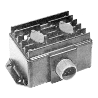
regulator. Transistors
Q6
and Q7 are high
power
types and
are
mounted on
a
finned
heat sink.
This
series pass
element
is rated at 8
amps
maximum
current capability.
Amplifier
Gain:
The
voltage
regulator unit shown
in Figure
3-5
is
basically
a
high
gain
voltage amplifier with a specially designed
narrow
dynamic range. The high gain is obtained by employing
the
common
emitter
configuration for
Q3,
Q4 and Q5,and
by keeping the
emitter
impedances as
low
as
possible. The net result
is
an amplifier
that
will limit in either
direction with
very
small chanyes
in input voltage
(at
the base
of
Q3).
3-9