— 25 —
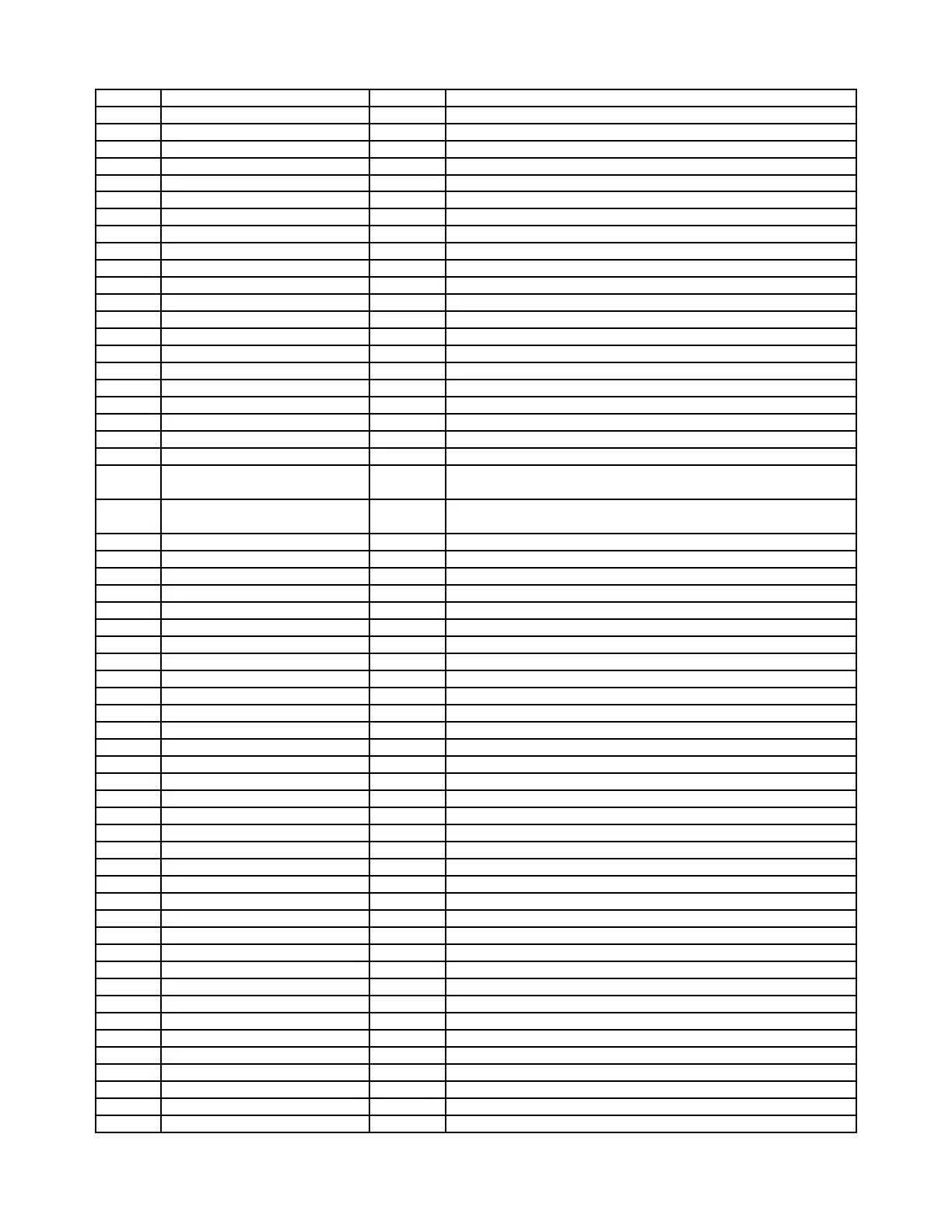
PIN NO. PIN NAME I/O DESCRIPTION
60 A13 O Address bus
61 VssQ - Input/output power supply (0 V)
62 A14 O Address bus
63 VccQ - Input/output power supply (3.3 V)
64 A15 O Address bus
65 A16 O Address bus
66 A17 O Address bus
67 A18 O Address bus
68 A19 O Address bus
69 A20 O Address bus
70 A21 O Address bus
71 Vss - Internal power supply (0 V)
72 A22 O Address bus
73 Vcc - Internal power supply (1.9 V)
74 A23 O Address bus
75 A24 O Address bus
76 A25 O Address bus
77 BS/PTC[0] O/IO Bus cycle start signal/input/output port C
78 RD O Read strobe
79 WE0/DQMLL O D7-D0 select signal / DQM (SDRAM)
80 WE1/DQMLU/WE O D15-D8 select signal / DQM (SDRAM)/write strobe (PCMCIA)
81 WE2/DQMUL/ICIORD/PTC[1] O/O/O/IO
D23-D16 select signal / DQM (SDRAM) / PCMCIA input/output
read/input/output port C
82 WE3/DQMUU/ICIOWR/PTC[2] O/O/O/IO
D31-D24 select signal / DQM (SDRAM) / PCMCIA input/output
write/input/output port C
83 RD/WR O Read/write
84 VssQ - Input/output power supply (0 V)
85 CS0 O Chip select
86 VccQ - Input/output power supply (3.3 V)
87 CS2/PTC[3] O/IO Chip select 2 / input/output port C
88 CS3/PTC[4] O/IO Chip select 3 / input/output port C
89 CS4/PTC[5] O/IO Chip select 4 / input/output port C
90 CS5/CE1A/PTC[6] O/O/IO Chip select 5 / CE1 (area 5 PCMCIA)/input/output port C
91 CS6/CE1B/PTC[7] O/O/IO Chip select 6 / CE1 (area 6 PCMCIA)/input/output port C
92 CE2A/PTD[6] O/IO Area 5 PCMCIA CE2 / input/output port D
93 VssQ - Input/output power supply (0 V)
94 CE2B/PTD[7] O/IO Area 6 PCMCIA CE2 / input/output port D
95 VccQ - Input/output power supply (3.3 V)
96 RASL/PTD[0] O/IO Lower 32 Mbytes address RAS (SDRAM) / input/output port D
97 RASU/PTD[1] O/IO Upper 32 Mbytes address RAS (SDRAM) / input/output port D
98 CASL/PTD[2] O/IO Lower 32 Mbytes address CAS (SDRAM) / input/output port D
99 CASU/PTD[3] O/IO Upper 32 Mbytes address CAS (SDRAM) / input/output port D
100 CKE/PTD[4] O/IO CK enable (SDRAM) / input/output port D
101 IOIS16/PTD[5] I/IO IOIS16 (PCMCIA) / input port D
102 BACK O Bus acknowledge
103 BREQ IN Bus request
104 WAIT IN Hardware wait request
105 DACK0/PTE[0] O/IO DMA acknowledge 0 / input/output port E
106 DACK1/PTE[1] O/IO DMA acknowledge 1 / input/output port E
107 DRAK0/PTE[2] O/IO DMA request acknowledge / input/output port E
108 DRAK1/PTE[3] O/IO DMA request acknowledge / input/output port E
109 AUDATA[0]/PTF[0] IO AUD data / input/output port F
110 AUDATA[1]/PTF[1] IO AUD data / input/output port F
111 AUDATA[2]/PTF[2] IO AUD data / input/output port F
112 AUDATA[3]/PTF[3] IO AUD data / input/output port F
113 AUDSYNC/PTF[4] O/IO AUD synchronous / input/output port F
114 TDI/PTG[0] IN Data input (H-UDI) / input port G
115 Vss - Internal power supply (0 V)
116 TCK/PTG[1] IN Clock (H-UDI) / input port G
117 Vcc - Internal power supply (1.9 V)