— 33 —
■ LCD INTERFACE
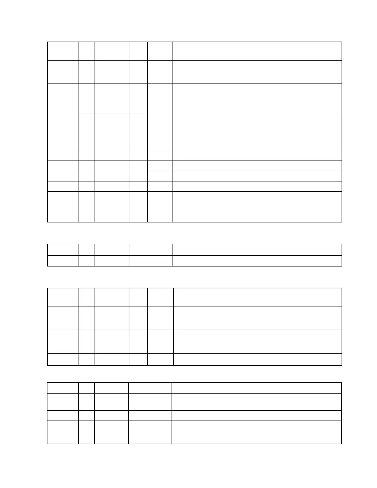
Pin Names Type Pin# Cell RESET# Description
State
30, 31, 32,
FPDAT[7:0] O 33, 34, 35, CN3 0 Panel Data
36, 37
These pins have multiple functions.
• Panel Data bits [10:8] for TFT/D-TFD panels.
FPDAT O, 24, 25, 26 CN3 Input • General Purpose Input/Output pins GPIO[3:1].
[10:8] IO These pins should be connected to IO V DD when unused.
This pin has multiple functions.
• Panel Data bit 11 for TFT/D-TFD panels.
FPDAT11 O, 23 CN3 Input • General Purpose Input/Output pin GPIO4.
IO • Inverse Video select pin.
This pin should be connected to IO V DD when unused.
FPFRAME O 39 CN3 0 Frame Pulse
FPLINE O 38 CN3 0 Line Pulse
FPSHIFT O 28 CN3 0 Shift Clock
LCDPWR O 43 CO1 0 Active high LCD Power Control
This pin has multiple functions.
• TFT/D-TFD Display Enable (DRDY).
DRDY O 42 CN3 0 • LCD Backplane Bias (MOD).
• Second Shift Clock (FPSHIFT2).
■ MISCELLANEOUS
Pin Names Type Pin# Cell RESET# Description
State
These inputs are used to configure the S1D13705 - see Table
CNF[3:0] I 46, 47, C As set by 5-1: “Summary of Power On/Reset Options,” on page 22.
48, 49 hardware Must be connected directly to IO V
DD
or V
SS
.
This pin has multiple functions - see REG[03h] bit 2.
GPIO0 IO, 22 CS/ Input • General Purpose Input/Output pin.
ITS1• Hardware Power Save.
TESTEN I 44 TEST
pulled low
Test Enable input. This input must be connected to V
SS
.
■ CLOCK INPUT
Pin Names Type Pin# DRIVER Description
CLKI I 51 C Input Clock
■ POWER SUPPLY
Pin Names Type Pin# DRIVER Description
COREVDD P 1, 21, 41, P Core V
DD
61
IOVDD P 10, 29, 52 P IO V
DD
20, 27, 40,
VSS P 50, 60, 72, P Common V
SS
80