— 5 —
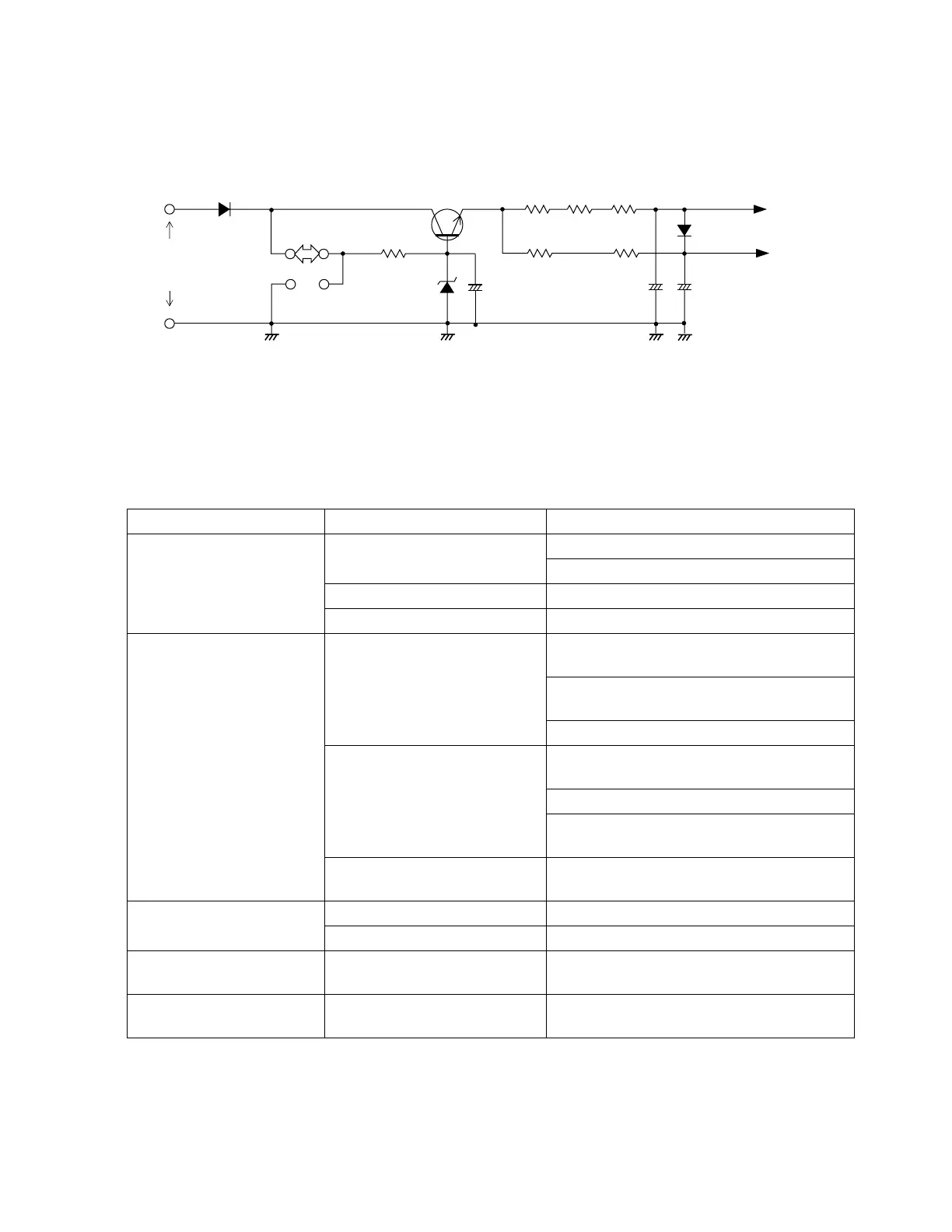
Power Supply Circuit
The power supply circuit regulates a constant output voltage +5.6V by T1 and D4.
R3 R4
R5
R37
D2
ON
OFF
Power Switch
DC +7.5 V
Input
GND
DGGND
AG
T1
2SD1858Q,R
D4
MTZJ6.8A
C3
R2
R6
C5
C4
D5
VDD +5.6V
AVDD +5.6V
Nature of Trouble Faulty Block Checkpoint
No power Power Supply Circuit Base of T1 should receive +6 V.
Emitter of T1 should provide +5.6 V.
Power switch Switch contact.
Power Jack (J1) Jack contact.
No sound at all Power Amp.
(IC1: AN8053N)
Pin 16 should receive +7.5 V when the
power switch is turned on.
Voltage at pin 14 should drop at 0V
when the power switch is turned on.
Check output signal of pin 1.
CPU (LSI1: MSM6521-11) Voltage at pin 27 should rise 0V to 5.6V
when the power switch is turned on.
Pins 39 ~ 46 should provide pulses.
Pin 29 should have a sound signal when
a key is pressed.
Oscillator (XL1) Pins 20 and 21 of the CPU should
receive an ocsillation signal.
Keyboard LEDs don't
light up
Keyboard LED
Keyboard LED Matrix Open circuir on LX or LY line.
A certain key or switch
does not function
Key and Switch Matrix Dust on the contact.
Certain keys or switches
do not function
Key and Switch Matrix Open circuit on KC or KI line.
TROUBLESHOOTING