— 10 —
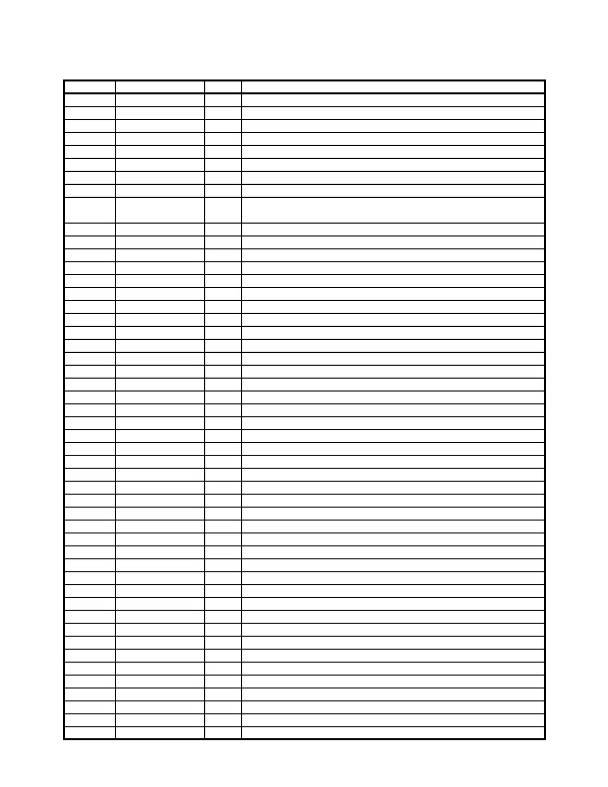
Pin No. Name I/O Function
1 VSS — Digital ground for LSI2
2~15 A10~A23 I/O Address bus
16 CS2 O Chip select to static RAM(LSI4)
17 CE3R O Chip enable to PS-RAM(LSI5)
18 CE3G O Chip enable to PS-RAM(LSI6)
20 RFSH O Refresh signal to PS-RAM(LSI5,6)
21 PSOE O Output enable to PS-RAM(LSI5,6)
22~29 DR0~DR7 I/O Data bus for PS-RAM(LSI5)/color data(red & green)
30~31,
34~39
DG0~DG7 I/O Data bus for PS-RAM(LSI6)/color data(blue) & work data
32 VSS — Digital ground for LSI2
33 VDD I Power supply for LSI2
48 SO1 O Serial data for thermal head(upper part of picture)
49 PCLK1 O Clock for thermal head(upper picture)
50 SO2 O Serial data for thermal head(lower part of picture)
51 PCLK2 O Clock for thermal head(lower picture)
52 LTCH O Latch pulse for data to thermal head
53 PSTB1 O Strobe signal for upper picture data to thermal head
54 PSTB2 O Strobe signal for lower picture data to thermal head
58 VDD I Power supply for LSI2
59 VSS — Digital ground for LSI2
60~72 Analog terminal — (not used)
73 VDD I Power supply for LSI2
74 VSS — Digital ground for LSI2
75 Analog terminal — (not used)
76 PON I Forced power on
77 POFF I Forced power off
78~80 Analog terminal I (not used)
85 TCON O Control for power(VP)(power on/off)
86 RSO O Reset output from LSI2
87 RSI I Reset signal to LSI2
88 VDE I Detection of low voltage(VDD1=4.30~4.35 V)
94~95 INT1~0 O Interrupt signal for LSI1(CPU)
96 VSS — Digital ground for LSI2
97 VDD I Power supply for LSI2
98 BUSGT I Bus grant signal from CPU(LSI1)
99 BUSRQ O Bus request to LSI1(CPU)
100 RESET O Reset signal to LSI1(CPU)
101~108 CD7~CD0 I/O Data bus
109 CWR I Write signal from LSI1(CPU)
110 CRD I Read signal from LSI1(CPU)
111 SYSCLK I System clock from LSI1(CPU), 6 MHz
112 VSS — Digital ground for LSI2
113 XIN I Master clock for LSI2(input), 24 MHz
114 XOUT O Master clock for LSI2(output), 24 MHz
115 VDD I Power supply for LSI2
116 CRFSH I Refresh signal from LSI1(CPU)
117 CLK O Clock for LSI1(CPU)
118~127 A0~A9 I/O Address bus
128 VDD I Power supply for LSI2
GATE ARRAY (MN7A076KYL): LSI2 (Internal analog circuit of LSI2 is not used)