— 21 —
22
23
24
25
26
27
28
1
2
3
4
5
6
7
21
20
19
18
17
16
15
14
13
12
11
10
9
8
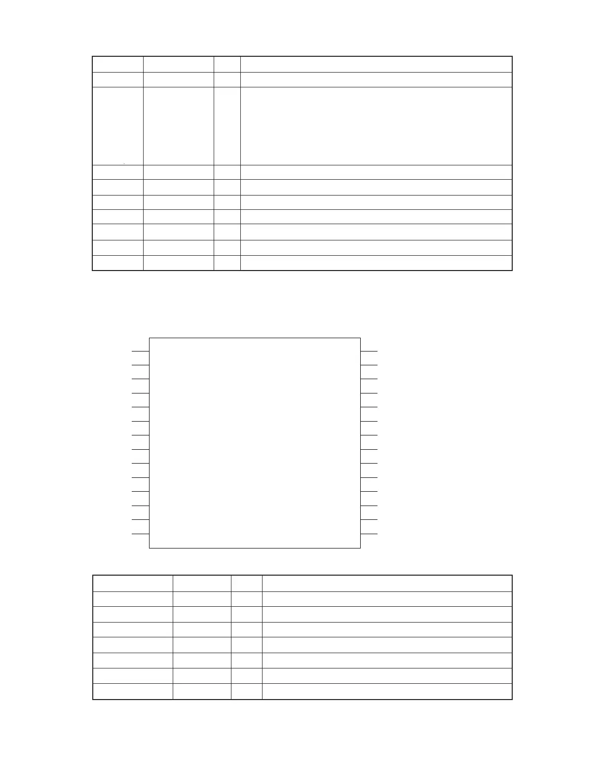
OE–
A11
A9
A8
A13
WE–
VCC
A14
A12
A7
A6
A5
A4
A3
A10
CE–
IO8
IO7
IO6
IO5
IO4
GND
IO3
IO2
IO1
A0
A1
A2
CXK58257ATM
(LSI 2)
7-2. RAM: LSI2 and LSI3 (CXK58257)
Pin No. Name I/O Description
64,65 OSC I/O I/O Clock terminal
67,69~71 V1 ~ 4 Voltage for LCD drive
OFF: 0 V ON– V1: 0.64 Minimum ~ 1.29 Maximum V
V2: 1.29 Minimum ~ 2.56 Maximum V
V3: 3.99 Minimum ~ 2.71 Maximum V
V4: 4.64 Minimum ~ 3.99 Maximum V
68 NC - Not used
72 INTO In Low battery detection INTO < 5.2 V => No power on
73 STNT In Power supply terminal (+5.3 V)
74 VLCD In Power supply terminal (+5.3 V)
S0 ~ 95 Out Segment signal for display
C5 ~ 32 Out Common signal for display
168,200 NC - Not used
172 ~199
75 ~ 171
Pin No. Name I/O Description
1~10,21,23~26 A0 ~ 14 In Address bus
11~13,15~19 IO1 ~ IO8 I/O Data bus
14 GND In GND 0 V
20 CE In Chip select signal from LSI1
22 OE In 0 V
27 WE In Write enable signal from LSI1
28 VCC In Power supply terminal (+ 5.3 V)
 Loading...