- 7 -- 7 -
- 7 -- 7 -
- 7 -
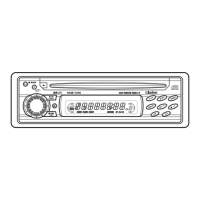
DB345MP/DB346MPDB345MP/DB346MP
DB345MP/DB346MPDB345MP/DB346MP
DB345MP/DB346MP
1 IPF OUT O IP flag output
2 SB OK O O Sub code Q data CRCC OK
signal output
3 CLOCKIO I/O The clock pulse input/output for
the sub code reading
4 VDD - Positive supply voltage
5 VSS - Nagative supply voltage
6DATA ODATA
7 SF SY O O Playback frame synchronous
signal output
8 SB SY O O Sub code block sychronous
signal output
9 HSO O The play speed flag ouput
10 UHSO O The play speed flag output
11 AR SEL IN I Fix to the high level
12 AWRC O The control signal ouput for the
active wide range VCO
13 P VDD - PLL positive supply voltage.
14 PDO O Phase difference signal output of
EFMPLCK.
15 TMAX S O T max judgment output.
16 TMAX O T max judgment output.
17 LPF N I Inverted input of LPF for PLL.
18 LPF OUT O The output terminal for the Low
Pass Filter.
19 P Vref - PLL reference voltage.
20 VCO FILTER O Loop filter for VCO.
21 VCO Ref I VCO reference voltage input.
22 DTC N O For the analog slicer.
23 DTC P O For the analog slicer.
24 PLL VSS - PLL ground.
25 SLCO O Output of internal DAC for data
slice level generation.
26 RF IN I RF signal input.
27 RF RP I RF ripple input.
28 RF EQ OUT O The output of the RF equalizer.
29 A VDD - Positive supply voltage for the
Analog section.
30 RES IN - For reference current setting.
31 Vref OUT O The reference voltage output.
32 VMDIR O The reference voltage output.
33 TESTR O The compensation terminal for
RFEQO offset.
34 INVSEL I MDI polarity selection.
35 AGCI I The input terminal of RF AGC
amplifier.
36 RF DCI I The input terminal for RF peak
detection.
37 RF OUT O RF signal output.
TC94A15F 051-6399-00
CD Mechanism IC
Outward FormOutward Form
Outward FormOutward Form
Outward Form
100 pins, plastic QFP
Terminal Description
38 PN SEL I The transistor type selection
input for laser diode driver.
L=NPN, H=PNP.
39 EQ SET O The equalizer setting terminal.
40 RF VDD - RF power supply.
41 LDO O The laser diode drive output.
42 MDI I Monitor photo diode signal input.
43 RF VSS - RF ground.
44 FNI 2 I Main beam signal input.
45 FNI 1 I Main beam signal input.
46 FPI 2 I Main beam signal input.
47 FPI 1 I Main beam signal input.
48 TPI I Sub beam signal input.
49 TNI I Sub beam signal input.
50 FTEO O For test.
51 RF ZI I RF ripple zero cross signal input.
52 A VSS - Analog ground.
53 RF RP O RF ripple signal output.
54 RF DC O RF peak detection signal output.
(hologram suitable)
55 FEI O Focus error signal output.
56 SBAD O Sub beam add signal output.
57 TEI O Tracking error signal output.
58 TE Z IN I Tracking error signal inpur for
zero cross.
59 A VDD - Positive supply voltage for the
Analog section.
60 FOO O Focus equalizer output.
61 TRO O Tracking equalizer output.
62 Vref O Reference voltage output.
63 FMO O Field equalizer output / Speed
error output.
64 DMO O Disk equalizer output.
65 IO2A I/O General input/output.
66 IO3A I/O General input/output.
67 MONIT O Internal DSP signal monitor.
68 FG IN I FG input for the spindle CAV
servo.
69 VSS - Negative supply voltage.
70 VDD - Positive supply voltage.
71 TESIN I For test.
72 X VSS - Master clock analog ground.
73 X IN I Crystal connection.
74 X O O Crystal connection.
75 X VDD - Clock power supply.
76 D VSS - Digital ground.
Pin No PIN NAME I/O DESCRIPTIONPin No PIN NAME I/O DESCRIPTION

 Loading...